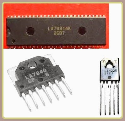
Service Mode _ working principle _ Voltage Chart to IC pins - Color TV circuit using ICs LA76814 and LC863424
SERVICE MODE
> Press PRO button to enter the adjustment or setup mode.
> Press CH+ or CH- button to turn page up or down for desired item options.
If a special remote controller is used for options, part of adjustment items can be selected directly by pressing buttons on the remote controller.
> Press VOL+ or VOL- button to alter the value of selected adjustment items.
In the factory production process, the factory adjuster is used for accelerated adjustment.
DEFAULT [FACTORY-SET] DATA
WORKING PRINCIPLE
MF amplifying circuit
Received by antenna and processed by the high frequency tuner, the television signals will be transmitted by the tuner as 45.75MHZ signals to sound surface filter through C112 coupling after being amplified by V102, and then the MF signals of trapped wave in sound carrier wave from sound surface filter F45U will be sent to pin 5 and 6 of LA76814. The MF demodulation circuit of this TV set is completed through PLL carrier wave generator and outside pressure control oscillator (T101) in LA76814. The MF frequency is adjusted by T101 adjustment, and output of AFC is generated by a numerical control IF-PLL circuit, and read and sent to CPU by I2C bus for correction of MF signals frequency deviation. The external capacitor of pin 3 decides the time constant of AGC, and high frequency application AGC will be transmitted by I2C bus through pin 4 for control of high frequency tuner gain.
Received by antenna and processed by the high frequency tuner, the television signals will be transmitted by the tuner as 45.75MHZ signals to sound surface filter through C112 coupling after being amplified by V102, and then the MF signals of trapped wave in sound carrier wave from sound surface filter F45U will be sent to pin 5 and 6 of LA76814. The MF demodulation circuit of this TV set is completed through PLL carrier wave generator and outside pressure control oscillator (T101) in LA76814. The MF frequency is adjusted by T101 adjustment, and output of AFC is generated by a numerical control IF-PLL circuit, and read and sent to CPU by I2C bus for correction of MF signals frequency deviation. The external capacitor of pin 3 decides the time constant of AGC, and high frequency application AGC will be transmitted by I2C bus through pin 4 for control of high frequency tuner gain.
Sound signals processing
The secondary sound MF signals are input via Pin 54 of LA76814, and then demodulated in PLL tuner through low pass and limit inside LA76814. After demodulation, the sound signals will be amplified through inside low pass and transmitted via Pin1. Pin 2 is FM output, C121 is de-accentuation capacitor, Pin 9 is FM detector’s DC filter connector and C117 is filter capacitor. The external AUDIO signals are input via LA76814 Pin 51, controlled by CPU. A switch inside I2C bus control LA76814 can be used for options of internal and external signals. The sound signals are transmitted via LA76814 Pin 1 to LA4225A Pin 1 via C601 coupling and transmitted from its Pin 4, after being amplified by LA4225A, to the speaker. The mute circuit 1 is comprised of V601, V602 and other components for Power On and Off mute. Circuit 2 is comprised of CPU mute Pin V603 and other components.
The secondary sound MF signals are input via Pin 54 of LA76814, and then demodulated in PLL tuner through low pass and limit inside LA76814. After demodulation, the sound signals will be amplified through inside low pass and transmitted via Pin1. Pin 2 is FM output, C121 is de-accentuation capacitor, Pin 9 is FM detector’s DC filter connector and C117 is filter capacitor. The external AUDIO signals are input via LA76814 Pin 51, controlled by CPU. A switch inside I2C bus control LA76814 can be used for options of internal and external signals. The sound signals are transmitted via LA76814 Pin 1 to LA4225A Pin 1 via C601 coupling and transmitted from its Pin 4, after being amplified by LA4225A, to the speaker. The mute circuit 1 is comprised of V601, V602 and other components for Power On and Off mute. Circuit 2 is comprised of CPU mute Pin V603 and other components.
Line sync processing circuit
The line oscillation circuit of the TV set is fully comprised of LA76814 internal integrated components. The brightness signals containing compound sync signals are transmitted to the internal sync separation circuit for line and field sync pulse.
The line oscillation circuit of the TV set is fully comprised of LA76814 internal integrated components. The brightness signals containing compound sync signals are transmitted to the internal sync separation circuit for line and field sync pulse.
Field sync and output circuit
Field sync separator produces field sync signals from compound sync signals and activates the field frequency splitting system. When a certain number field sync pulse is detected, the field frequency splitting system will start operation for frequency splitting of the multiple line frequency signals generated by the line frequency oscillator. The field pulse gained from frequency splitting will be sent to field saw tooth generator for saw tooth waves, and then transmitted by Pin 23. The output circuit of this TV set is mainly comprised of LA7840 and other components.
Field sync separator produces field sync signals from compound sync signals and activates the field frequency splitting system. When a certain number field sync pulse is detected, the field frequency splitting system will start operation for frequency splitting of the multiple line frequency signals generated by the line frequency oscillator. The field pulse gained from frequency splitting will be sent to field saw tooth generator for saw tooth waves, and then transmitted by Pin 23. The output circuit of this TV set is mainly comprised of LA7840 and other components.
Line output circuit
Standard line oscillation pulse is output via Pin 27 to V431 for line drive. T431 is H (L) drive used to convert the low current and high pressure pulse signals from line tube into low voltage and large current signals for line export needs. V432 is line output, C435 and C436 are reciprocal capacitor, C441 is S calibration capacitor, L441 is line linear inductance and T471 is line output transformer. 240V voltage needed for field scanning is transmitted via winding 10 of the transformer and gained after being rectified by VD472. In addition to anode high pressure, screen grid and focus voltages, the transformer provides 180V video amplifier voltage by winding 2. VD411, C411, R412, VD412, R414 and C412 form the X ray protection circuit. R233, C231, R232, R403 and C408 form the beam restriction circuit. The winding 9 of the transformer provides CRT filament voltage.
Standard line oscillation pulse is output via Pin 27 to V431 for line drive. T431 is H (L) drive used to convert the low current and high pressure pulse signals from line tube into low voltage and large current signals for line export needs. V432 is line output, C435 and C436 are reciprocal capacitor, C441 is S calibration capacitor, L441 is line linear inductance and T471 is line output transformer. 240V voltage needed for field scanning is transmitted via winding 10 of the transformer and gained after being rectified by VD472. In addition to anode high pressure, screen grid and focus voltages, the transformer provides 180V video amplifier voltage by winding 2. VD411, C411, R412, VD412, R414 and C412 form the X ray protection circuit. R233, C231, R232, R403 and C408 form the beam restriction circuit. The winding 9 of the transformer provides CRT filament voltage.
CRT output circuit
The tricolor signals produced by LA76814 will be transmitted to CRT board and then to the cathode of the TV tube after being amplified by video amplifier which is comprised of V902, V912 and V922.
The tricolor signals produced by LA76814 will be transmitted to CRT board and then to the cathode of the TV tube after being amplified by video amplifier which is comprised of V902, V912 and V922.
CCD performance
The CVBS signals produced by LA76814 pin 40 will be amplified and sent to N701 pin 19 via V821 and then processed by software and hardware inside CPU. The decoded CCD signals will be transmitted to LA76814 pin 14, 15 and 16 via CPU pin 22, 23 and 24.
The CVBS signals produced by LA76814 pin 40 will be amplified and sent to N701 pin 19 via V821 and then processed by software and hardware inside CPU. The decoded CCD signals will be transmitted to LA76814 pin 14, 15 and 16 via CPU pin 22, 23 and 24.
V-CHIP performance
Performance of V-CHIP is mainly completed by CPU. The CPU receives grade signals from the IC bus and executes relative performances and shields those programs of relative grade.
Performance of V-CHIP is mainly completed by CPU. The CPU receives grade signals from the IC bus and executes relative performances and shields those programs of relative grade.
All integrated circuit voltages
Following voltage data is achieved while the TV set is turned on, and the electric resistance is achieved when the TV set is turned off. When the status changes, the data should also be changed. So these data are used as references.
Following voltage data is achieved while the TV set is turned on, and the electric resistance is achieved when the TV set is turned off. When the status changes, the data should also be changed. So these data are used as references.
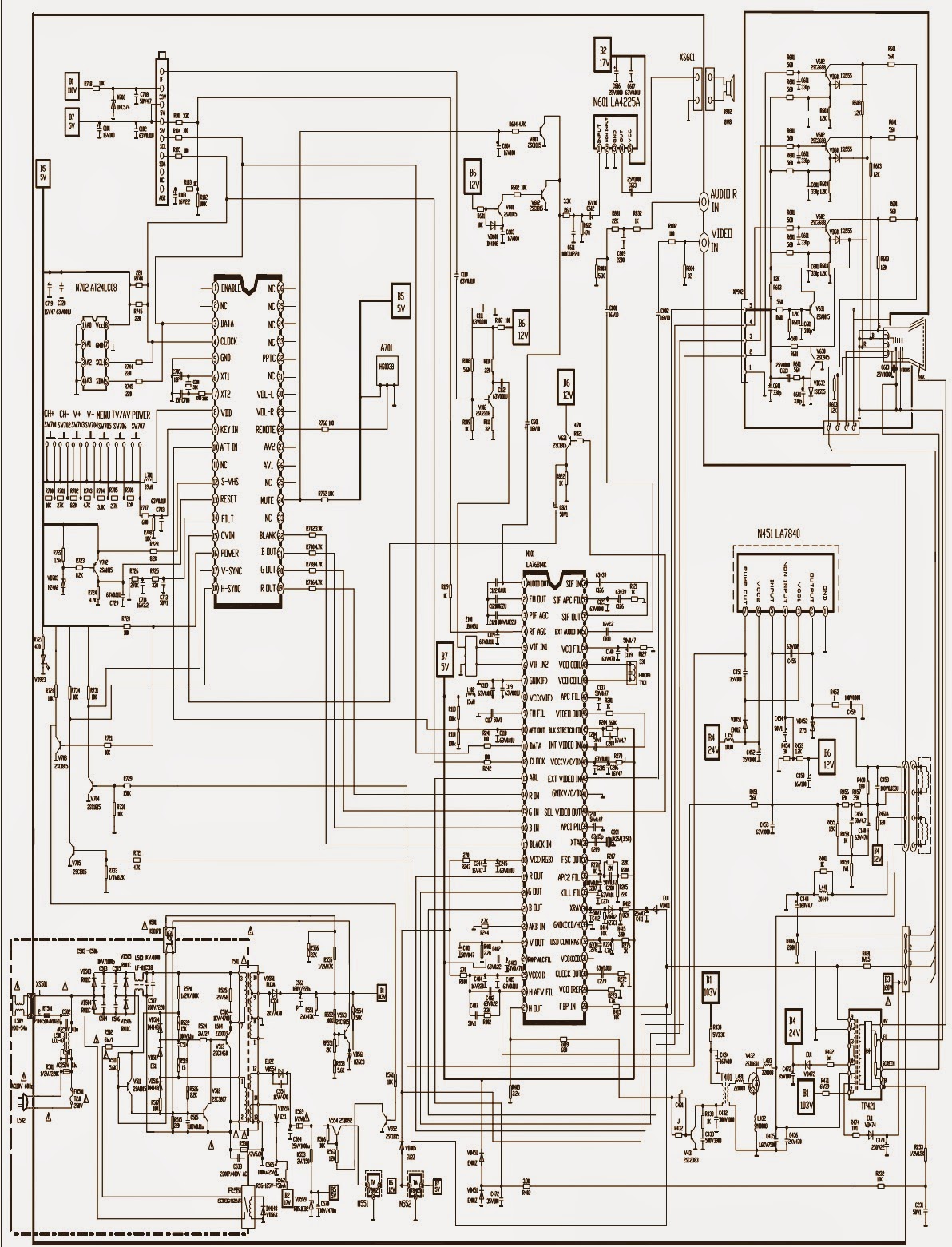
CIRCUIT DIAGRAM (SCHEMATIC) HAIER
CLICK ON THE PICTURES TO ZOOM IN


