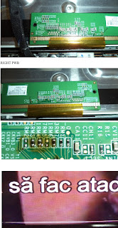
PANEL SCREEN: LTF320AP11, T-Con S100FAPC2LV0.3, Processor: BD8193MWV, Gamma MAX9694E
Panel screen used in Samsung LE32D450G1W TV
VONE value=28v, VOFFE= -11,5v
Gain signals CKV1, CKVB1, CKV2, CKVB2 and STVP are outputted to screen cell thru 4 resistors, 0 ohms, as in image below.
Panel screen used in Samsung LE32D450G1W TV
VONE value=28v, VOFFE= -11,5v
Gain signals CKV1, CKVB1, CKV2, CKVB2 and STVP are outputted to screen cell thru 4 resistors, 0 ohms, as in image below.
When all image is colorless or with hue of green/red pale, the fault is from NVM Eeprom, 24C64WP. Replace it, with another one, write it before solder. A very often fault found with this type of panel - image is ok only on lower part of the screen, and upper side is discolored and full of visible horizontal lines, as in picture below.
The reason for this fault, is a fried connection of a SR gate block, from left/right side of the screen (check after you remove the metal rim that covers the screen)
The repair procedure: The fault starts after a few minutes, when faulty SR gate run too hot, so you can add a thermal sponge pressed by metal rim, or you can cut the signals CKV1, CKVB1, CKV2, CKVB2 and STVP only on fault side.PANEL SCREEN LTJ400HM07, T-CON S100FAPC2L v0.3 (BN41-01687A)
Fault: The thin horizontal stripes at the top of the screen. Cause of the defect: burned SR block in the higher right/left corner of the panel
Repair procedure: Disconnect left FFC between T-con and left PWB and power the tv. If you have now on right part of the screen a normal image, means that you have a fault in left side of the cell. If still a fault image, re-connect the left FFC and disconnect right FFC between T-con and left PWB and power the tv. If you have now on left part of the screen a normal image, means that you have a fault in right side of the cell. On the right side (with problems) resistors RM2, RM3, RM4, RM5 RM6 and RM7
You will have a normal picture now, but sometimes, you will have, on side with problems, a little ODD/EVEN lines distance. Strap with a wire, on check points, CKV1 with CKVB1, see if lines are now correct displayed. If not, strap with a wire, on check points CKV2 with CKVB2, check, and repeat procedure with CKV3 with CKVB3. Now you will have a clean image. Sometimes, if you have a bigger problem on SR circuit, the image will be correct but a / some thin line (s) will be displayed sometimes on screen, noticeable on lighter/darker images. Check if any improvements if connect all pairs of check points on fault side on GND or Voff.
PANEL SCREEN LTF400HM03, T-CON S100FAPC2L v0.3
Fault: 15 - 30 minutes of good image, begins to trembling, double vertically. If you check on strips of glass with your fingers, you will find that hot broken drivers are on one of the the left/right bar.
Repair procedure: Disconnect left/right FFC cable between T-con and left/right PWB one by one, and check which part is fault. Remove on pairs (CKV1 and CKVB1 and so on), the 7 resistors from fault side RM1-RM7. If needed, strap pairs coming from screen, on check points (CKV1 with CKVB1, CKV2 and CKVB2, and so on) You can also try to strap pairs to GND or Voff and see if better picture.
On example below, was enough to cut CKV1-CKVB1 pair on fault side, by removing corresponding resistors, and the image came back to normal.
Some thin lines can appear sometimes. Just Strap CKV1-CKVB1 pair, and connect it to GND or VSS, and the lines will disappear.
PANEL SCREEN LSF320HJ01, T-CON: 2013_TCON_FOX_FT1 (BN41-01939)
FAULT: Horizontal lines on partial/ all screen
Repair procedure: Disconnect one by one the left/right FFC cable between T-con and left/right PWB and start the tv, this way you can easy check which part is fault. Level shifter IC is connected to left/right gate blocks, thru some zero ohms resistors fitted on T-con, thru left/right FFC cable, thru left/right PWB and extreme left/right flexible data driver circuit
The clock signal pairs CKV1-CKVB1, CKV2-CKVB2, CKV3-CKVB3 and start signal STVP have check points on each side, but they are covered with paint and are very close to PCB's through-holes, so cutting the circuits is an hard operation.
The easiest way to repair the panel is to cut all 7 signal connectors from FFC cable, only on the side with fault, on TCON side. If any horizontal thin lines remains over normal displayed image, clean the paint from check points on PWB side with fault, and strap with a wire the pair check points CKV1- CKVB1, see if lines disappeared. If not, connect the strapped to GND or Voff. Repeat procedure with pairs CKV2-CKVB2, and CKV3-CKVB3 for best results.


