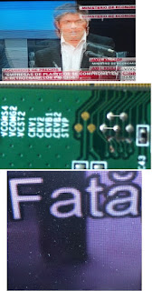
PANEL SCREEN LTY320AP04 and LTZ320AP04, TCON:320AP04S4LV1.5 and 320AP04S4LV1.7
FAULT: Image trembling, double vertically, horizontal lines on all/partial screen.
FAULT: Image trembling, double vertically, horizontal lines on all/partial screen.
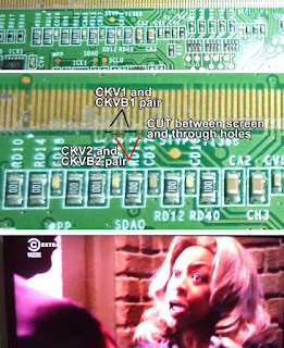
T-CON board is not detachable, and signals to left/right gate blocks, is transmitted thru left/right flexible data driver circuits. So, it's almost impossible to check which gate is fault. Usually, the right part faults more often, so you can start to disconnect signals from there. You must cut the connections between PCB's through-holes and check points, so the check points to remain connected to panel, as in picture.
Disconnect first the pair CKV1-CKVB1 and STVP and power the tv and check if any improvement. If not, try to strap CKV1-CKVB1. Check again. Try to connect CKV1- CKVB1 to GND. Disconnect the pair CKV2-CKVB2 and and power the tv and check if clear display. If not, try to strap CKV2-CKVB2. Try to connect CKV2-CKVB2 to GND.If CKV2-CKVB2 faults, try to rebuild connection for pair CKV1-CKVB1. Your goal is to have best image you can achieve. Sometimes a thin horizontal line will be displayed, even you have a perfect image. You can not eliminate this failing. The line is not noticeable from normal view distance, but it's position depends on the position of faulty SR gate block. On image bellow, the line is very close to lower part of the screen.
PANEL SCREEN LTA400HW03 J, TCON: SH120PMB45V0.3
FAULT: Image trembling, double vertically, horizontal lines on all/partial screen.
FAULT: Image trembling, double vertically, horizontal lines on all/partial screen.
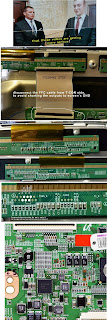
Disconnect left FFC between T-con and left PWB and power the tv. If you have now on right part of the screen a normal image, means that you have a fault in left side of the cell. If still a fault image, re-connect the left FFC and disconnect right FFC between T-con and left PWB and power the tv. If you have now on left part of the screen a normal image, means that you have a fault in right side of the cell. On upper image, there is a problem in the right side gate screen driver.
On the side with problems, remove from PWB the resistors RM1-RM7, in this order: first remove the CKV1 and CKVB1 resistors RM2 and RM5 and see any improvements. If not, remove CKV2 and CKVB2 resistors RM2 and RM6, check if any improvements, and if not, remove CKV3 and CKVB3 resistors RM3 and RM7. If still no improvements, remove STVP resistor, RM1 see picture.
You will have a normal picture now, but sometimes, you will have, on side with problems, a little ODD/EVEN lines distance. Strap with a wire, on check points, CKV1 with CKVB1, see if lines are now correct displayed. If not, strap with a wire, on check points, CKV2 with CKVB2, check, and repeat procedure with CKV3 with CKVB3. In example bellow, the pair CKV3-CKVB3 was strapped Connect check points by pair, but only if corresponding resistors were removed, or else you can burn the LEVEL SHIFTER IC from T-CON
Sometimes, will be better to put back the resistors for the blocks pair that have no problem. For example if only by disconnecting CKV3 and CKVB3 will solve image problem, that means pair 1 and 2 have no problems. Sometimes, if you have a bigger problem on cell circuit, the image will be correct but a / some thin line (s) will be displayed sometimes on screen, noticeable on lighter/darker images. Try to connect the pair that not work on GND or Voff. You can also raise Voff voltage with 3-5 volts to minus and the line will disappear. You have to do this on T-con Board, by raising the value of the resistor connected between FBN input of BiasPS/Level shifter ICD1 – RT9979 and VOFFE.
PANEL SCREEN LSY320AN02, TCON: 320KSB_S2LV0.2
Screen is flickering, have a part/all the screen with doubled image, white ghosting on part / all screen
T-CON board is not detachable, and signals to left/right gate blocks, is transmitted thru extreme left/right flexible data driver circuit. It's only one data driver flexible circuit, so, it's almost impossible to check which gate is fault (left/right).
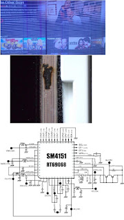
But sometimes, if you detach and reverse the cell glass, you will see burned circuits on glass, so you can now know which side is fault. There are several connections that you have to cut on fault side: CKV1-CKVB1, CKV2-CKVB2, Vss, Vcom and Vcst The LEVEL SHIFTER is integrated in DC-DC source drive IC2 – RT69068, or SM4151. The IC's have same configuration, the only difference is the Vreff voltage (pin18) 3,3V or 5v.
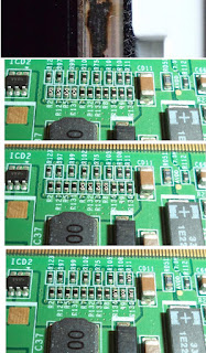
The connections from LEVEL SHIFTER and left/right gate blocks are made thru some 10 ohms resistors, RD10, RD14, RD9, RD11, RD13, RD12 and RD40, as in picture. CKV1 and CKV2 have 2 outputs on each side to double the current and to avoid LEVEL SHIFTER overheating.
REPAIR PROCEDURE.
On fault side, you must cut the connections to left/right side, between PCB's through-holes and panel, so the check points to remain connected to working side of the panel, as in picture. PCB's through-holes, connects the other side of the cell with gate signals, so cutting the connections between resistors and through-holes, will cut signals on both sides of the screen.
If no burned circuits on reverse side of the cell, first try to find out which pair creates problems on screen. First, remove RD10, RD14 and RD,13 and check if CKV1- CKVB1 pair creates problems. If not, solder back the resistors, and remove RD9, RD11 and RD 12, and see if CKV2-CKVB2 pair creates problems. Cut only pair with problems, as in picture:
It's a very difficult procedure. Do not try it if you don't have a microscope or a power magnifier lens.
Now you will have a clean and almost perfect image.
Now you will have a clean and almost perfect image.
PANEL SCREEN: LTJ400HM05, T-Con 400HR42S4LV0A, 400HR42S4LV0B
Screen is flickering, have a part/all the screen with doubled image, upper side is discolored and have visible horizontal lines
First step is to find which part of the screen is fault.
This operation is very hard, the t-con is attached to cell glass thru data drivers. We don't have resistors on CKV-CKVB left-right pair signals, so we have to make a big effort to find out where is the fault. If you have a point where fault starts, you can try to see if a burned SR block can be seen on fault side.
You can detach and reverse the cell glass, you will see burned circuits on glass, so you can now know which side is fault. There are several connections that you have to cut on fault side: CKV1-CKVB1, CKV2-CKVB2, CKV3-CKVB3, STVP
This operation is very hard (the screen is 40 inches), so do not try this if you don't have 2 clean and large tables, covered with some bubble wrap or white paper.
If you cannot see any burned blocks, even with a microscope or magnifier, follow this steps:
1. Remove resistors R2, R127, R5 and R131 (zero ohms) for pair CKV1-CKVB1 that connects LEVEL SHIFTER IC with both left-right SR blocks. R2 and R127 are connected parallel for CKVB1 signal. R5 and R131 are in parallel connection for CKV1. You can find the resistors in the left side of level shifter IC – SM4109, as in image below:
Power the tv and check if any improvements on screen. If not, solder back the resistors from 1st pair and remove CKV2 and CKVB2 resistors R7+R132 and R8+R133, power up the tv and check if any improvements.
If still no change, solder back the resistors from 2nd pair and remove CKV3 and CKVB3 resistors R9+R134 and R11+R136.
2.We know now which pair creates the fault on screen, solder back all resistors and let's find on what side (left or right) is the defective SR block. If, for example CKV1-CKVB1 pair is fault, we will disconnect the signal from left side of the screen (if you could see with a magnifier where is the fault, cut connections on fault side)
We will disconnect left side because we have more space to re-connect the signals if there is no problem on this side, and the fault is on the right side.
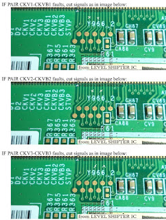
Cut the signals corresponding that goes on left side of the screen:
We will disconnect left side because we have more space to re-connect the signals if there is no problem on this side, and the fault is on the right side.
Cut the signals corresponding that goes on left side of the screen:
There is a 50 % chance that the left side of the cell to be fault. If the image is ok now, but some thin line (s) will be displayed on screen, noticeable on lighter/darker images, try to connect the pair that not work on GND or Voff.
ATTENTION! Connect the fault screen inputs to GND, only if this inputs were disconnected from LEVEL SHIFTER IC, as in image bellow. Just clean with a cutter IF PAIR CKV1-CKVB1 faults, cut signals as in image below:
Just clean with a cutter the green paint from upper side that goes in screen and solder a thin wire from GND to both inputs. Now the SR blocks are closed by connecting to GND, the analog gate outputs from fault side will be opened, and the lines will disappear from the image.
Before connecting the power, check with diode measurement instrument for any shorts from outputs of LEVEL SHIFTER IC to GND (check on all re-soldered resistors and GND)
On left side, we have check points for all LEVEL SHIFTER signals CKV-CKVB1-3 signals. Lower PCB's through-holes, are connected with back circuits to LEVEL SHIFTER IC. On upper PCB's through-holes are connected all signals to right side of the cell:
If the right side is fault, we have to re-connect the left inputs of the screen to signals and cut the right side of corresponding pair signals.
On example below, if CKV1-CKVB1 pair faults, on left side clean with a cutter the paint where initially were cut the signals, add some thermal paste and solder a thin wire.
Also, cut the signals from right side from back of the t-con PCB or near right inputs as in images.
