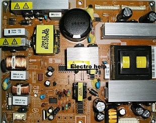
The BN44-00192A is used on Samsung LCD TVs with a diagonal size of 26 and 32 inches.
The circuit can be divided into the following areas:- Power Factor Corrector (PFC or PFC - Power Factor Correction);
- Power supply;
- Work energy source;
Consider the circuits of these nodes in more detail.
Power Factor Correction
The Power Factor Correction (PFC) serves to eliminate the harmonics in the input circuit that the Rectifier diodes make together with the electrolytic capacitor of the IIP network rectifier filter.
In the absence or malfunction of the PFC and the input filters, the current in the rectifier network is only at short intervals of the capacitor load time, when the amplitude value of the voltage is equal to the voltage in the capacitor and the current consumed takes the form of short pulses with amplitude of several amps.
Details of current distortion and Power Factor (CM or PF - Power Factor) in rectifiers are considered on the page of a full-wave rectifier.
Due to the negative effects of harmonics in the electrical network, manufacturers incorporate a PFC circuit, active or passive depending on the power, according to the European standard of electrical compatibility EN 61000-3-2 for Class D devices.
As a result of the operation of the PFC module of the active device BN44-00192, the current in the input is forced by the LP801 blocker, the QP801S electrical switch and the DP802 diode, which are the of the step-up converter.
The switch is controlled by the ICP801S PWM controller and, in addition to providing a stable output capacitor, generates a current during the period in the form of a set of short pulses whose amplitude is determined taking into account the internal multiplier (multiplexer) of the input and output.
In this case, the line of received current pulses repeats the form of the rectified grid voltage applied at the 100 Hz frequency applied to the accelerator. The frequency of the current pulses generated by the device is within tens of kilohertz and is partially filtered by the CP801 0.47 uF capacitor at the PFC input.
Finally, the highest current harmonics are separated from the network by an input filter using two parallel coils. As a result, the current in the input circuit acquires a shape close to the sinusoidal and the power factor of the power module becomes close to 100%.
The PFC device is connected simultaneously with the working power supply, changing the voltage M_Vcc on pin 8 of the ICP801S controller. In the standby mode, the active PFC does not work and the rectified grid voltage (+311 V) of the diode bridge passes through the diode DP801 to the filter capacitor. With low loads, there are input filters sufficient to filter the harmonics, which are essentially passive PFC (CMC)
Standby power.
The unit is implemented according to the controller controlled flyback converter scheme PWM ICB801S. The drive operates at a fixed frequency of 55-67 kHz and generates a stable 5.2 V at the output with a load current of up to 0.6 A to power the control processor in the PWM chips from the main source and PFC in the operating mode.
The transition from the standby mode of the TV to the working mode is carried out by switching the 5.2 V the transistor switch QB802. In this case, the supply voltage M_Vcc goes to the controllers PWM ICP801S and ICM801, simultaneously initiating the PFC node and the main power supply.
Operational power supply
The source is a front transducer made by a half bridge circuit and generates the following voltages stabilized on output:
24 V to turn on the inverter display.
13 V.
12 V.
5.3 V for Main_Board supply, obtained by means of the 24 V rectifier step-down converter.
Typical malfunctions
Known popular defects of this module are:
- Malfunction of secondary rectifier filter capacitors.
- Crack formation in the welds of transistor QB802, which connects the M_Vcc power supply of the standby mode.
Less common defects:
- Disaggregation of working source switch transistors (QM801, QM802) and breaker resistor RM801 due to a mode violation when working with faulty capacitors from its secondary rectifiers.
- Overheating of the aforementioned key transistors due to the malfunction of the capacitor CM801 of the master oscillator PWM due to a change in frequency of the inverter operation.
Circuit diagram (Schematic) - Click on the pictures to magnify


