Quantcast
Channel: Electro help
Viewing all 2033 articles
Browse latest View live

Sony HCD DAV S500 - How to open the disc tray when power switch turns off or during a power failure –, How to disassemble Disc mechanism

$
0
0
HCD-S500/S800 are the amplifier, DVD/CD and tuner section in DAV-S500/S800

How to eject the disc tray when power switch is turned off, or during a power failure
When removing the disc tray, high torque is necessary to turn the ejection cam on the bottom surface. Therefore, the screw thread is easily damaged. To prevent this damage, turn it carefully.
How to disassemble the disc mechanism - Sony HCDS500 – S800
RF 240 board, Tray and KHM240AAA Optical pickup
When disassembling the Tray, push the two protrusions, release the two claws fixing the tray and pull out the tray in the direction of the arrow A. (Be careful of the two claws.)
OPTICAL PICK-UP - KHM-240AAA


Sony DAV-S500-DAV-S800 – Compact AV system - SMPS and Amplifier section schematic [Circuit diagram]

$
0
0
Abbreviation
AUS : Australian model
E32 : 110-240V AC area in E model(MODELO BR)
EA : Saudi Arabia model
HK : Hong Kong model
MY : Malaysia model
SP : Singapore model
US Model, Canadian Model, Chinese Model - DAV-S500

AEP Model, UK Model, Australian Model, E Model - DAV-S500/S800
SMPS schematic
SMPS PWB
Amplifier schematic and PWB
Click on the pictures to magnify

HCD DAV-S500 - S800 Sony COMPACT AV SYSTEM Test mode and adjustment details

$
0
0
Self-diagnosis Function
When the self-diagnosis function is activated to prevent the system from malfunctioning. In this case a five-character service number (e.g., C 13 00) with a combination of a letter and digits appears on the screen and the front panel display.
TEST MODE
VERSION DISPLAY MODE
Procedure:
1. Press the EJECT  button on the main unit or POWER button on the remote commander to turn the set on.
2. Press three buttons of FUNCTION , . PREV and EJECT simultaneously for two seconds.
3. The message “VER. 1. ** ” is displayed for a moment.
JOG TEST MODE
Procedure:
1. Press the EJECT button on the main unit or POWER button on the remote commander to turn the set on.
2. Press three buttons of BAND , STOP and EJECT simultaneously.
3. The fluorescent indicator displays “JOG 0”. The value “JOG 0” increases like +1, +2, +3... if rotating the VOLUME knob clockwise ,or it decreases like –1, –2, –3,.... if rotating counterclockwise.
4. To exit from this mode, press the POWER button to turn the set off.
KEY TEST MODE
Procedure:
1. Press the EJECT button on the main unit or POWER button on the remote commander to turn the set on.
2. Press three buttons of DISPLAY , STOP and EJECT simultaneously.
3. The message “KEY NUM 0” is displayed and “0” blinks.
4. Each time a button is pressed, “KEY NUM 0” value increases.  However, once a button is pressed, it is no longer taken into account.
5. When all buttons are pressed, “KEY NUM 11” appears and the number blinking is stopped.
6. To exit from this mode, press the POWER button to turn the set off.

DISPLAY TEST MODE
Procedure:
1. Press the EJECT button on the main unit or POWER button on the remote commander to turn the set on.
2. Press three buttons of BAND , PAUSE and EJECT simultaneously.
3. All segments are turned on.
6. Press the NEXT > button, all segments are turned off.
7. Every pressing of the NEXT > button turns on each segments in the same order.
8. To exit from this mode, press the POWER button to turn the set off.
OSD TEST MODE
Procedure:
1. Press the EJECT button on the main unit or POWER button on the remote commander to turn the set on.
2. Set the FUNCTION to DVD.
3. While pressing two buttons of DISPLAY and STOP simultaneously, turn the VOLUME knob clockwise.
4. The Test Mode Menu is displayed on the TV screen.
5. To execute each function, select the number on the remote commander.
6. See the following section for explanation in detail.
7. To exit from this mode, press the POWER button to turn the set off.
DISC TRAY LOCK
Procedure:
1. Press the EJECT button on the main unit or POWER button on the remote commander to turn the set on.
2. Press two buttons of DISPLAY and . PREV simultaneously for two seconds.
3. The message “LOCKED” is displayed and the tray is locked.
(Even if exiting from this mode, the tray is still locked.)
4. Press two buttons of DISPLAY and . PREV simultaneously for two seconds again.
5. The message “UNLOCKED” is displayed and the tray is unlocked.
6. To exit from this mode, press the POWER button to turn the set off.
The Test Mode allows you to make diagnosis and adjustment easily using the remote commander and monitor TV. The instructions, diagnostic results, etc. are given on the on-screen display (OSD).
STARTING TEST MODE
Set the FUNCTION to DVD with the main unit power on. Next, while pushing the STOP button and the [DISPLAY] button on the main unit at the same time, turn the VOLUME knob to the right to start
Test Mode and display the menu shown below on the TV screen. At the bottom of the menu screen, the model name and revision number are displayed.
To execute each function, select the desired menu and press its number on the remote commander. To exit from Test Mode, press the [POWER] button.

SYSCON DIAGNOSIS
The same contents as board detail check by serial interface can be checked from the remote commander.
On the Test Mode Menu screen, press [0] key on the remote commander, and the following check menu will be displayed.
Quit
Quit the Syscon Diagnosis and return to the Test Mode Menu.
All
All items continuous check
This menu checks all diagnostic items continuously. Normally, all items are checked successively one after another automatically unless an error is found, but at a certain item that requires judgment through a visual check to the result, the following screen is displayed
for the key entry.
For the ROM Check, the check sum calculated by the Syscon is output, and therefore you must compare it with the specified value for confirmation.
Following the message, press [NEXT] key to go to the next item, or [PREV] key to repeat the same check again. To quit the diagnosis and return to the Check Menu screen, press STOP or [ENTER] key. 
If an error occurred, the diagnosis is suspended and the error code is displayed.
Press STOP key to quit the diagnosis, or [PREV] key to repeat the same item where an error occurred, or [NEXT] key to continue the check from the item next to faulty item.
Selecting 2 and subsequent items calls the submenu screen of each item.
For example, if “5. Supply” is selected, the following submenu will be displayed.
0. Quit
Quit the submenu and return to the main menu.
1. All
All submenu items continuous check
This menu checks 2 and subsequent items successively. At the item where visual check is required for judgment or an error occurred, the checking is suspended and the message is output for key entry.
Normally, all items are checked successively one after another automatically unless an error is found.Selecting 2 and subsequent items executes respective menus and outputs the results.
General Description of Checking Method
Version
Revision
ROM revision number is displayed.-
Error: Not detected.
The revision number defined in the source file of ROM (At the beginning of mass production, the Flash ROM of IC107 is used, but midway it is replaced by the IC108 OTP ROM.IC107 or IC108) is displayed with four digits.Below IC107 are all IC107 or IC108.
ROM Check Sum
Check sum is calculated.
Error: Not detected.
The 8-bit data are added at addresses 0x000F0000 ~ 0x002EFFFF of ROM (IC107) and the result is displayed with 4-digit hexadecimal number. Error is not detected.
 Model Type
Model code is displayed.
Error: Not detected.
The model code read from EEPROM (IC101) is displayed with 2-digit hexadecimal number.
 Region
Region code is displayed.
Error: Not detected.
The region code determined from the model code is displayed.
Peripheral
EEPROM Check
Data write > read, and accord check
Error 03: EEPROM write/read discord
Data 0x9249, 0x2942, 0x4294 are written to addresses 0x00~0xFF of EEPROM (IC101), then read and checked.
Before writing, the data are saved, then after checking, they are written to restore the contents of EEPROM.
Servo
Servo DSP Check
Data write -> read, and accord check
Error 12: Read data discord
Data 0x9249, 0x2942, 0x4294 are written to the address 0x602 of RAM in the Servo DSP (IC302), then read and checked.
DSP Driver Test
Test signal data → DSP Driver
Error: Not detected.
Caution: Do not conduct this test with a mechanical deck connected.
The maximum voltage is applied to the Servo Driver IC (IC401, IC802). If mechanical deck is connected, the motor and optics could be damaged. Disconnect mechanical deck following the output message, then enter specified 4-or 5-digit number from the remote commander, and press the [ENTER]. 
The test is conducted only when the input data accord. Check the output level, then press the [NEXT] to finish the test.
This test is skipped if “All” is selected.
Supply
Caution: Do not conduct this check with a mechanical deck connected.
An access is made to the stream supply and servo control IC (IC302) and external RAM (IC303) using check data.
If mechanical deck is connected, the motor and optics could be damaged. This check is also executed by the “All” menu item.
ARP Register Check
Data write => read, and accord check
Error 08: ARP register write, and read data discord
Data 0x00 to 0xFF are written to the TMAX register (address 0xC6) in ARP (IC302), then they are read and checked.
ARP to RAM Data Bus
Data write => read, and accord check
Error 09: ARP <-> RAM data bus error Data 0x0001 to 0x8000 where one bit each is set to 1 are written to the address 0 of RAM (IC303) connected to the ARP (IC302) through the bus, then they are read and checked.
In case of discord, written bit pattern and read data are displayed. If data where multiple bits are 1 are read, the bits concerned may touch each other. Further, if data where certain bit is always 1 or 0 regardless of written data, the line could be disconnected or shorted.
ARP to RAM Address Bus
Data write => other address read discord check
Error 10: ARP → RAM address bus error
Caution: Address and data display in case of an error is different from the display of other diagnosis (described later).
Before starting the test, all addresses of RAM (IC303) are cleared to 0x0000.
First, 0xA55A is written to the address 0x00000, and the address data are read and checked from addresses 0x00001 to 0x80000 while shifting 1 bit each. Next, the data at that address is cleared, and it is written to the address 0x00001, and read and checked in the same manner. This check is repeated up to the address 0x80000 while shifting the address data by 1 bit each.
If data other than 0 is read at the addresses except written address, an error is given because all addresses were already cleared to 0. In this check, the error display pattern is different from that of other diagnosis; read data, written address, and read address are displayed in this order. However, the message uses same template, and accordingly exchange Address and Data when reading.
ARP RAM Check
Data write → read, and accord check
Error 11: ARP RAM read data discord The program code data stored in ROM are copied to all areas of RAM (IC303) connected to the ARP (IC302) through the bus, then they are read and checked if they accord. If the detail check was selected initially, the data are
written to all areas and read, then the same test is conducted once again with the data where all bits are inverted between 1 and 0. If discord is detected, faulty address, written data, and read data are displayed following the error code 11, and the test is suspended.
AV Decoder
1930 RAM
Data write => read, and accord check
Error 13: AVD RAM read data discord
The program code data stored in ROM (IC107 or IC108) are copied to all areas oo»RAM (IC504, IC505) connected to the AVD (IC503) through the bus, then they are read and checked if they accord. Further, the same test is conducted once again with the data where all bits are inverted between
1 and 0. If discord is detected, faulty address, written data, and read data are displayed following the error code 13, and the test is suspended.
930 SP
ROM => AVD RAM → Video OUT
Error: Not detected.
The data including sub picture streams in ROM (IC107 or IC108) are transferred to the RAM (IC504, IC505) in AVD (IC503), and output as video signals from the AVD (IC503).
They are output from all video terminals (Composite, Y/C).
Video
Color Bar
AVD color bar command write => Video OUT
Error: Not detected.
The command is transferred to the AVD, and the color bar signals are output from video terminals.
They are output from all video terminals (Composite, Y/C).
DRIVE AUTO ADJUSTMENT
On the Test Mode Menu screen, press [1] key on the remote commander, and the drive auto adjustment menu will be displayed.
 Normally, [0] is selected to adjust DVD (single layer), CD, DVD (dual layer), and SACD in this order. But, individual items can be adjusted for the case where adjustment is suspended due to an error.
In this mode, the adjustment can be made easily through the operation following the message displayed on the screen.
The disc used for adjustment must be the one specified for adjustment. However, for SACD disc, use the player with initial data if the disc is not available.
ALL
Select [0] and press [ENTER] key, and the servo set data in EEPROM will be initialized. Then, 1. DVD-SL disc, 2. CD disc, 3. DVD-DL disc, and 4. SACD disc are adjusted in this order. Each time one disc was adjusted, it is ejected. Replace it with the specified disc following the message.
 Though the message to confirm whether discs other than SACD disc are adjusted is not displayed, you can finish the adjustment if pressing the STOP button. During adjustment of each disc, the measurement for disc type judgment is made. As automatic adjustment does not judge the disc type unlike conventional models, take care not to insert wrong type discs. Also, do not give a shock during adjustment.
CD
Select [2], insert CD disc, and press [ENTER] key, and the adjustment will be made through the following steps, then adjusted values will be written to the EEPROM.
CD Adjustment Steps
1. Sled Tilt Rest
2. Disc Check Memory CD
3. Wait 500 msec
4. Set Disc Type CD
5. LD ON
6. Spdl Start
7. Wait 500 msec
8. Focus Servo ON 0
9. Auto Track Offset Adjust
10. CLVA ON
11. Wait 500 msec
12. Tracking ON
13. (TC Display Start)
14. Wait 1 sec
15. Jitter Display Start
16. Sled ON
17. Check CLV ON
18. Auto LFO Adjust
19. Auto Focus Offset Adjust
20.
21. Auto Focus Gain Adjust
22. Auto Focus Offset Adjust
23. Eq Boost Adjust
24. Auto LFO Adjust
25. Auto Track Gain Adjust, Search Check
26. 32Tj Fwd
27. 32Tj Rev
28. 500Tj Fwd
29. 500Tj Rev
30. All Servo Stop
DVD-SL (single layer)
Select [1], insert DVD single layer disc, and press [ENTER] key, and the adjustment will be made through the following steps, then adjusted values will be written to the EEPROM.
DVD Single Layer Disc Adjustment Steps
1. SLED TILT Reset
2. Disc Check Memory SL
3. Wait 300 msec
4. Set Disc Type SL
5. LD ON
6. Spdl Start
7. Wait 1 sec
8. Focus Servo ON 0
9. Auto Track Offset Adjust
10. CLVA ON
11. Wait 500 msec
12. Tracking ON
13. Wait 1 sec
14. Sled ON
15. Check CLV Lock
16. Auto LFO Adjust
17. Auto Focus Offset Adjust
18. Auto Tilt Position Adjust
19. Auto Focus Gain Adjust
20. Auto Focus Offset Adjust
21. EQ Boost Adjust
22. Auto LFO Adjust
23. Auto Track Gain Adjust, Search Check
24. 32Tj Fwd
25. 32Tj Rev
26. 500Tj Fwd
27. 500Tj Rev
28. All Servo Stop
29. Eep Copy Loop Filter Offset.
DVD-DL (dual layer)
Select [3], insert DVD dual layer disc, and press [ENTER] key, and the adjustment will be made through the following steps, then adjusted values will be written to the EEPROM.
DVD Dual Layer Disc Adjustment Steps
1. Sled Tilt Reset
2. Disc Check Memory DL
3. Wait 500 msec
4. Set Disc Type DL
5. LD ON
6. Spdl Start
7. Wait 1 sec, Layer 1 Adjust
8. Focus Servo ON 0
9. Auto Track Offset Adjust
10. Clva ON
11. Wait 500 msec
12. Tracking ON
13. Wait 500 msec
14. Sled ON
15. Check CLV Lock
16. Auto Loop Filter Offset Auto Focus Adjust
17.
18. Auto Focus Gain Adjust
19. Auto Focus Offset Adjust
20. Eq Boost Adjust
21. Auto Loop Filter Offset
22. Auto Track Gain Adjust, Search Check
23. 32Tj Fwd
24. 32Tj Rev
25. 500Tj Fwd
26. 500Tj Rev, Layer 0 Adjust
27. Fj (L1 -> L0)
28. Auto Track Offset Adjust L0
29. Clva ON
30. Wait 500 msec
31. Tracking ON
32. Wait 500 msec
33. Sled ON
34. Check CLV Lock
35. Auto Focus Filter Offset
36. Auto Focus Adjust
37.
38. Auto Focus Gain Adjust
39. Auto Focus Offset Adjust
40. Eq Boost Adjust
41. Auto Loop Filter Offset
42. Auto Track Gain Adjust, Search Check
43. 32Tj Fwd
44. 32Tj Rev
45. 500Tj fwd
46. 500Tj Rev, Layer Jump Check
47. Lj (L0 -> L1)
48. Lj (L1 -> L0)
49. All Servo Stop.
LCD
Select [4], insert SACD disc, and press [ENTER] key, and the adjustment will be made through the following steps, then adjusted values will be written to the EEPROM. However, if SACD disc is not available, use the player with initial data, skipping the SACD adjustment. In this case, you can finish the adjustment if pressing the stop button.
SACD Adjustment Steps
1. Sled Tilt Reset
2. Set Disc Type CD
3. LD ON
4. Spdl Start
5. Wait 500 msec
6. Focus Servo ON 0
7. Auto track Offset Adjust
8.
9. CLVA ON
10. Wait 500 msec
11. Tracking ON
12. Wait 1 sec
13. Sled ON
14. Check CLV ON
15. Auto Focus Offset Adjust
17.
18. Auto Focus Gain Adjust
19. Auto Focus Offset Adjust
20. Eq Boost Adjust
21. Auto LFO Adjust
22. Auto Track Gain Adjust
23. 32Tj Fwd
24. 32Tj Rev
25. 500Tj Fwd
26. 500Tj Rev
27. All Servo Stop */
MECHA AGING
On the Test Mode Menu Screen, selecting [3] executes the aging of the mechanism. Start aging with PLAY. During aging, the repeat cycle is displayed. Aging can be aborted at any time by pressing the STOP key. After the operation is stopped, press the STOP key or [RETURN] key again to return to the Test Mode Menu. SEARCH Aging is only for a CD.

Sony KLV32V530A, KLV40V550A, KLV46V550A, KLV52V550A – LCD TVs – How to enter service mode, LED blinking codes – SMPS schematic

$
0
0
KLV-40V550A RM-GA015 - India, Iran, ME, Philippines, Russia, South Africa, Thailand, Tunisia
KLV-40V550A/R RM-GA015 - ME, Philippines, (Red) Thailand, South Africa
KLV-40V550A/W RM-GA015 - ME, Philippines, (White) Thailand, South Africa
KLV-46V550A RM-GA015 - India, ME, Philippines, Russia, South Africa, Thailand
KLV-52V550A RM-GA015 - India, Iran. ME, Philippines, Russia, South Africa, Thailand, Tunisia
KLV-32V550A/R RM-GA015 - ME, Philippines,
KLV-32V530A KLV-32V550A RM-GA015 - ME
RM-GA015 - India, ME, Philippines, Russia, South Africa, Thailand, Tunisia
SERVICE ADJUSTMENTS
Viewing Service Adjustment Data
There are no adjustments necessary for these models.  All data have been set for optical viewing for customers.
Accessing Service Adjustment Mode
1. While TV on standby, press the following sequence on the remote commander
[i] On screen display] +[ 5 ] + Volume [+] + Power
The following menu appears on the screen. 
Use the following buttons on the remote commander to access the service menu:
To reset to factory default, press [8] > [Mute] > [0]
To exit, turn off and on the TV set.
Accessing Diagnostic Menu
While TV on standby, press the following sequence on the remote commander.
The following menu appears on the screen
To exit, turn off and on the TV set.
SELF DIAGNOSTIC FUNCTION
LED Pattern
When safety shutdown occurs, Standby LED display reports the cause by using the lightning patterns as indicated below.
LED Display Specification, LED Display Control, Standby LED Error Display and countermeasures according to Standby LED blinking times.
Power board PWB and Power board [G2BE] schematic
Click on the pictures to magnify

LG CM4730 Mini Hi-Fi System - No Power, No sound troubleshooting – SMPS and Maim amplifier schematic (circuit diagram)

$
0
0
LG CM4730 Mini Hi-Fi System  (CM4730, CMS4630F, CMS4530W) – Power and amplifier boards schematics, How to troubleshoot  No power, No sound - Hidden Key functions
HIDDEN KEY MODES
Push both Front key and RCU key to activate it for 5 seconds.
1. Disc Lock On/Off (CD Function Only Active)
Front Key : STOP
RCU Key : STOP
2. Check Version and Option code
Front Key : STOP
RCU Key : PLAY/PAUSE
You can change [Audio MCU Version <-> CD Controller Version <-> EEPROM Option] by SKIP+/-.
3. Clear EEPROM
Front Key : STOP
RCU Key : SKIP-
4. Edit EEPROM
Front Key : STOP
RCU Key : SKIP+
You can change the digit of option by SKIP+/-.
You can edit 0~f by REPEAT or PLAY/PAUSE key.
5. Bluetooth DUT
Front Key : STOP
RCU Key : PROGRAM
Bluetooth model only
6. Power Disc Lock On/Off (CD Function Only Active)
Front Key : STOP
RCU Key : EQ
7. Amp Clip On/Off
Front Key : STOP
RCU Key : Mute
Amp Clip Mode Change (Amp Clip On --> Amp Clip Off --> Level Down display).
8. Demo ALL Key Lock (CM9520/CM8520 Only)
Front Key : STOP
RCU Key : 9
Demo All Key Lock Change (All Key Lock On --> All Key Lock Off).
- Working on Demo Operation only.
- When All Key Lock, Volume Key work only.
- After All Key Lock Off, it can unlock Demo Mode.
PROGRAM DOWNLOAD & UPDATE
AUDIO PROGRAM
Download program file name must be CM4530_xxxxxxx.HEX
If security program (Water Wall) is activated on your PC, you must save the file to the USB storage device and disable the security software, then download the file to your set.
Caution: When downloading the file, you should neither unplug the USB device, change to the other function, nor power off the device. USB device must be unplugged when the downloading process is completed
CD PROGRAM
Download program file name must be HF000_CM4530_xxxxxxxx_xx.bin
Tip) With B/T : HF000_CM4530_xxxxxxxx_xx.bin
Without B/T : HF400_CM4530_xxxxxxxx_xx.bin
If security program (Water Wall) is activated on your PC, you must save the file to the USB storage device and disable the security software, then download the file to your set.
Caution: When downloading the file, you should neither unplug the USB device, change to the other function, nor power off the device. USB device must be unplugged when the downloading process is completed.
EQ PROGRAM
Download program file name must be EQ_PRG_CM4730_xxxxxxxxx_xxxx.bin
If security program (Water Wall) is activated on your PC, you must save the file to the USB storage device and disable the security software, then download the file to your set.
Caution: When downloading the file, you should neither unplug the USB device, change to the other function, nor power off the device. USB device must be unplugged when the downloading process is completed.
No Power - Troubleshooting
SMPS Schematic
SMPS PWB Component and foil sides
NO POWER
If the unit doesn’t work by no power problem, repair the set according to the following
FUSE & BRIDGE DIODE
Check and replace F901, BD901, TH901 on SMPS board.
1) Check if the fuse F901 is open or short-circuit.
2) Check if the bridge diode BD901 is short-circuit by over current with a digital multi meter.
3) Check if the NTC thermistor TH901 is normal or open.
D929
Check and replace D929 on SMPS board.
How to troubleshoot
1) Check the Anode-Cathode Voltage of D929 with a digital multi-meter, it is normally 0.2 ~ 0.3 V.   If it doesn’t have any voltage, it’s destroyed. Replace it with a new one.
NO SOUND
There is no sound output in the CD FUNCTION, repair the set according to the following 
IN THE CD FUNCTION
Check and replace IC601, IC801 on MAIN board.
How to troubleshoot 
1) Check CD_BCLK, CD_LRCK, & CD_DOUTA signals from IC302 to IC801.   If no signal, check if the RF & servo signals from MD is entered to IC302.
2) Check the following I2S signal flow. < I2S audio signal Interface >
- DAC_BCK : IC801_Pin85 --> IC601_Pin23
- DAC_LRCK : IC801_Pin86 --> IC601_Pin22 (44.1 kHz)
- DAC_DATA : IC801_Pin81 --> IC601_Pin24
- DAC_MCLK : IC801_Pin84 --> IC401_Pin44
If there is any trouble, check the power for each IC. The power is normal but, if the signal waveform to the IC is distorted or no signal, replace it with a new one.
3) Check if “Digital audio AMP block”. 
Main amplifier Schematic
NO SOUND
There is no sound output by DIGITAL AUDIO AMP DAMAGE, repair the set according to the following.
BY DIGITAL AUDIO AMP DAMAGE (IN ALL FUNCTIONS)
Check and replace IC701, IC702 on MAIN board.
How to troubleshoot (Countermeasure)
1) Check FL±, FR± & SW± signals from IC601 to IC701 & 702 each input function.   If no signal, check if I2S audio signals are entered to IC601.
2) Check PVDD.   If PVDD is abnormal, check the SMPS.
3) Check +12 V for driving the gate of AMP IC.
a. All the powers are normal, but if +12 V is low, there is possible for AMP IC to be damaged.
b. Remove L707, L708, L709 and L712 one by one.
When removed a inductance, if +12 V is recovered, the IC connected to it was damaged.
c. Replace the IC with a new one.
4) Check the impedance between IC701/IC702_OUT-A/OUT-B & GND.
a. If the impedance is 0 Ω, the IC must be damaged.
b. After removing the heat sink, replace it with a new one.
There is no sound output in the USB FUNCTION, repair the set according to the following.
IN THE USB FUNCTION
Check and replace IC801 on MAIN board & IC502 on USB board.
How to troubleshoot
1) Check +5VU to USB board.   If the USB LED are turned on, the voltage is okay, if so not, check +5.6 V to pin6 of CN502.
2) Check USB D± from MAIN board to USB board.
a. Check USB_DM/DP signals to IC801 (pin117, 118).
b. Check USB± signals to CN502 (pin1, 2, 4, 5).   If there is any trouble; check the power for each IC. The power is normal but , if the signal waveform to the IC is distorted or no signal, replace it with a new one.
3) Check if “Digital audio AMP block “normal.
There is no sound output in the AUX FUNCTION, repair the set according to the following guide.
IN THE AUX FUNCTION
Check and replace IC401 on MAIN board.
How to troubleshoot (Countermeasure)
1) Check AUX_L/R signals to IC401 (Pin7, 8).
2) Check if DAC_BCK, DAC_LRCK, & DAC_MCLK are entered from IC801 to IC401.
3) Check if ADC_DATA is entered from IC401 to IC801.   If no signal, check +5 V & +3.3 V(ADC) for IC401. If is NG, replace it a new one.
4) Check the following I2S signal flow from IC801 to IC602.  If there is any trouble, check the power for each IC. The power is normal but, if the signal waveform to the IC is distorted or no signal, replace it with a new one.
5) Check if the digital audio AMP block is okay.  If AMP is damaged, replace it with a new one.
There is no sound output in the TUNER FUNCTION, repair the set according to the following guide.
IN THE TUNER FUNCTION
Check and replace IC401, TU100 on MAIN board.
How to troubleshoot
1) Check if TUNER_LR is entered from Pin1,3 of TU100 to IC401(Pin23, 24).  If no signals, Check +3.3 V for Tuner power.  Check if the Tuner control signals (CLK, DAT, CE, RST, SLT) are entered from IC102 to TU100.
If it doesn’t work, replace TUNER with a new one.
2) Check if DAC_BCK, DAC_LRCK, & DAC_MCLK are entered from IC501 to IC401.
3) Check if ADC_DATA is entered from IC401 to IC801.  If no signal, check +5 V & +3.3 V(ADC) for IC401. If is NG, replace it with a new one.
4) Check the following I2S audio signal flow from IC801 to IC601. (Refer to Item 5-1.)  If there is any trouble, check the power for each IC. The power is normal but, if the signal waveform to the IC is distorted or no signal, replace it with a new one.
5) Check if the digital audio AMP block is okay.  If AMP is damaged, replace it with a new one.
Click on the pictures to magnify

PDI-P23LCD – PAL-SECAM-NTSC – 23 inch TFT LCD TV – How to enter the service mode, schematic diagram, functional description

$
0
0
Excessive heat applied to the copper foil of any printed circuit board will weaken the adhesive that bonds the foil to the circuit board causing the foil th separate from or “lift-off” the board.

The TFT LCD TV described in the followings is based on a Multi TV system, digital Control display, 23.01" diagonal. The TFT LCD TV is intended to be a finished product, basically a display device mounted inside an enclosure which will provide the safety Requirements. With the exception of LCD Panel, the display device shall be composed entirely of solid state components these components shall have a history of reliable service in identity applications and shall be applied in the circuits.
1. SCALER SECTION.
2. VCT 49xxi SECTION.
3. Video A/D Converter
How to enter, adjust and exit the service mode
When the EEPROM has been replaced, the SVC data should be restored as the function of individual system and specification.
When the EEPROM has been replaced White Balance Checking.
[ Enter and exit SVC mode ]
Note: into the SVC mode, Initialize with default data.
1) Press 5 Seconds MENU buttons on both TV set and Remote Controller at the same time to get into SVC mode.
2) Press the PR ▲▼ button several times to find SVC Data.
3) Input the corresponding SVC data referring to Table below with the VOL
◀▶ , key.
4) Press TV/AV button to exit SVC mode.
If the set is cold, there may be a small “flicker” when the set is switched on.  This is normal; there is nothing wrong with the set.
Some dot defects may appear on the screen, like Red,Green or Blue spots,  However, this will have no impact or effect on the monitor performance.
The resolution which is not supported will appear at the resolution which gets near to the resolution which is supported.
*The standard of the resolution which gets near : H/V sync.
Press the Q.VIEW button to switch the 640x480 60hz to 720x480P 60Hz
ADJUSTMENT INSTRUCTION WITH DEFAULT FACTORY DATA:White Balance Checking
Schematic  / [Circuit diagram]
Click on the pictures to magnify
SCALER SECTION
Device : MST6151
Features: Input supports up to UXGA & 1080P
Panel supports up to SXGA/WXGA
Integrated two-port triple-ADC/PLL
Integrated DVI/HDCP compliant receiver
YUV422 digital video input ports
Dual high-quality scaling engines
Built-in 3-D video de-interlacer
Video-over-graphic PIP
Video-by-graphic split screen
MStarACE advanced picture/color processing engine
Embedded On-screen Display Controller (OSD) engine
Built-in dual-link LVDS transmitter
5-Volt tolerant inputs
Low EMI and power saving features
Supports PWM & GPO controls
208-pin PQFP package
Analog RGB/YPbPr Input Ports
DVI/HDCP Compliant Input Port
Video Input Port
Auto-Configuration/Auto-Detection
Dual High-Performance Scaling Engines
Video Processing & Conversion
On-Screen OSD Controller
Description
The MST6151 is a high performance and fully integrated graphics processing IC solution for multi-function LCD monitor/TV with resolutions up to SXGA/WXGA. It is configured with an
integrated triple-ADC/PLL, an integrated DVI/HDCP receiver, a video de-interlacer, two high quality scaling engines, an on-screen display controller, and a built-in output clock generator. By use of external frame buffer, PIP is provided for multimedia applications. It supports de-interlaced full-screen video, video-on-graphic overlay, video-by-graphic split screen, frame rate conversion, and aspect ratio conversion for various video sources. To further reduce system costs, the MST6151 also integrates intelligent power management control capability for green-mode requirements and spread-spectrum support for EMI management.
VCT 49xxi SECTION
Device : VCT 49xxi
Features : PSSDIP88-1/-2 package
PMQFP144-2 package
Submicron CMOS technology
Low-power standby mode
Single 20.25-MHz reference crystal
8-bit 8051 instruction set compatible CPU
Up to 256 kB on-chip program ROM
WST, PDC, VPS, andWSS acquisition
Closed Caption and V-chip acquisition
Up to 10 pages on-chip teletext memory
Multi-standard QSS IF processing with single SAW
FM Radio and RDS with standard TV tuner
TV-sound demodulation:
Baseband sound processing for loudspeaker channel:
CVBS, S-VHS, YCrCb and RGB inputs
4H adaptive comb filter (PAL/NTSC)
multi-standard color decoder (PAL/NTSC/SECAM)
Nonlinear horizontal scaling “panorama vision”
Luma and chroma transient improvement (LTI, CTI)
Non-linear color space enhancement (NCE)
Dynamic black level expander (BLE)
Scan velocity modulation output
Soft start/stop of H-drive
Vertical angle and bow correction
Average and peak beam current limiter
Nonlinear and dynamic EHT compensation
Black switch off procedure (BSO)
Description
The VCT 49xxI is an IC family of high-quality single chip TV processors. Modular design and deep-submicron technology allow the economic integration of features in all classes of single scan TV sets. The VCT 49xxI family is based on functional blocks contained and approved in existing products like DRX 396xA, MSP 34x5G, VSP 94x7B, DDP 3315C and SDA 55xx.
Each member of the family contains the entire IF, audio, video, display, and deflection processing for 4:3 and 16:9 50/60-Hz mono and stereo TV sets. The integrated micro-controller is supported by a powerful OSD generator with integrated Teletext & CC acquisition including on-chip page memory.
control
*Integrated clamp with timing generator
*Integrated Brightness & Contrast controls
*Integrated precision voltage reference
*Compatible with VGA through SXGA RGB graphics signals, and component TV, DTV and HDTV
*Pin Compatible with AD9883A
*Serial port programming interface
*Mid-Scale Clamping
*Fully Sync Processing
*4:2:2 and 4:4:4 Output Format Mode
*Color space conversion (RGB to YCbCr)
*Internal pattern generator*
*Sawtooth vertical deflection signals for VSYNC input*
*BT656 output format mode*
*Black and mid-level precision clamp and calibration*
*Please see MST9883C Application Note for details.RGB Graphics
Processing
(A/D Converter):   Description
Most flat-panel monitors and projectors require a digital graphics input in order to accurately scale and display graphics. The huge installed base of computers with analog video graphics interfaces necessitates the use of a graphics digitizer to re-digitize the analog RGB signal before further processing.
 The MST9883CR is a fully integrated analog interface for digitizing high-resolution RGB graphics signals from PC’s and workstations. With a sampling rate capability of up to 140 MHz, it can accurately support display resolutions up to 1280x1024 (SXGA) at 75 Hz. The clamped input circuits provide sufficient band width to accurately digitize each pixel.
 The MST9883CR provides a high performance highly integrated solution to support the digitization process, including the ADC’s, a voltage reference, a PLL to generate the pixel sampling clock from HSYNC, clamping circuits, and programmable offset and gain circuits to provide brightness and contrast controls.
 When the COAST signal is asserted, the PLL will maintain its output frequency when HSYNC pulses are absent, such as during the VSYNC period in some systems.
 A 32-step programmable phase adjustment control (0-360 deg) is provided for the pixel sampling clock to adjust for the difference between the HSYNC edge and RGB pixel edge timing.
 The MST9883CR can send output data through one 24-bit port at the pixel clock rate.
 The MST9883CR can also support RGB to YCbCr conversion.
 The MST9883CR has internal programmable pattern generator for testing.
 The MST9883CR can accept either standard TTL, CMOS levels or saw tooth vertical deflection signals for VSYNC input.
Device: Features - MST9883CR
*Triple ADC with 12 - 140 MHz Sampling Rate
*Integrated line locked PLL generates pixel clock from HSYNC
*Integrated 5-bit pixel clock phase adjustment for precise sample timing.

Sanyo LCE32R83DT – how to enter the service mode, service adjustments, and software update procedure – LED LCD TV

$
0
0
Sanyo LCE32R83DT LED-LCD TV PAL/SECAM -B/G, D/K, I, NTSC(AV) - Power voltage test, software update, service mode, service adjustments
 The unit adjustments
 Connect power/backlight board assembly, data processing assembly, IR/Key board assembly correctly, supply with power, turn on the TV set.
Check display.
Factory menu instruction
a) Press key “INPUT”, press digital keys “2,5,8,0” in turn to enter into primary factory menu;
b) Press keys “UP ” and “Dn ” to move cursor to each page of primary factory menu, then press key “ENTER” to enter into submenu page;
c) Press keys “Up ” and “Dn ” to move cursor upward or downward within any one page;
d) Press keys “Left ” and “Right ” to do adjustment when move cursor to one item;
e) Press key “MENU” to exit submenu page of factory menu sequentially; The cursor must focus on the first item when pressing key “MENU” to exit some of the submenu page.
f) Factory menu item: Aging Mode to be used for aging the TV set when the option is “On”; press any key on key board to exit aging mode during the aging process;
g) Factory menu item: Other setting → Power on mode:
‘On’: to turn on the TV set with one step;
‘Off’: to turn on the TV set with two steps;
‘Last’: to keep the last power-off state when power on the TV set again;
Power voltage test
Connect the power board assembly, data processing assembly, IR/Key board assembly correctly, supply with power, press button standby to turn on the TV set.
Click on the table to magnify
White balance adjustment
Before adjustment
The TV set should be working above 30 minutes to be in a stabler state before adjustment. Use CA-210 BBY channel to adjust white balance;
a) VGA channel adjustment
Input square signal (VG848 Timing: 854 (VESA 800×600/60 Hz), enter into user menu SETTING→Computer Settings→ AUTO ADJUST to make picture display fully; then input signal (VG848 PAT: 914), enter into factory menu page ADC ADJUST to perform AUTO ADC until the prompt “SUCCESS” displays.
b) YPbPr channel adjustment
Input signal (VG848 Timing: 968 (480i/60 Hz) PAT: 918 (100% color bar + gray scale)) , enter into factory menu page ADC ADJUST to perform AUTO ADC until the prompt “SUCCESS” displays.
c) Only Normal color temperature needs adjusting for the model. Chromatic coordinates of bright scale must be set as (X=±5, Y=±5), chromatic coordinates of dark scale must be set as (X=±10, Y=±10).
Four groups of white balance adjustments
 DVI channel adjustment (HDMI,USB channel with the same adjustment method of this one)
Input signal (VG848 Timing: 854
PAT: 921 (16-gray-step)), enter into factory menu page Color Temp, fix item G-GAIN, adjust items R-GAINB-GAIN to set chromatic coordinates of the reversed 4th scale as the date of NORMAL; fix item G-OFFSET, adjust items R-OFFSETB-OFFSET to set chromatic coordinates of the 4th scale as the date of NORMAL; adjust items R-GAINB-GAIN and R-OFFSETB-OFFSET repeatedly as above until chromatic coordinates of both gray scales are the data of NORMAL;
Check if chromatic coordinates of WARM is (313329), if not, adjust items R GAIN / B GAIN / R OFF/ B OFF to be up to the requirements and then save the data.
Check if chromatic coordinates of COOL is (272
278), if not, adjust items R GAIN / B GAIN / R OFF/ B OFF to be up to the requirements and then save the data
VGA channel adjustment
Input signal (VG848 Timing: 854
PAT: 921 (16-gray-step)), enter into factory menu page Color Temp, fix item G-GAIN, adjust items R-GAINB-GAIN to set chromatic coordinates of the reversed 4th scale as the date of NORMAL; fix item G-OFFSET, adjust items R-OFFSETB-OFFSET to set chromatic coordinates of the 4th scale as the date of NORMAL; adjust items R-GAINB-GAIN and R-OFFSETB-OFFSET repeatedly as above until chromatic coordinates of both gray scales are the date of NORMAL;
Check if chromatic coordinates of WARM is (313329), if not, adjust items R GAIN / B GAIN / R OFF/ B OFF to be up to the requirements and then save the data.
Check if chromatic coordinates of COOL is (272
278), if not, adjust items R GAIN / B GAIN / R OFF/ B OFF to be up to the requirements and then save the data.
YPbPr channel adjustment
Input signal (VG848 Timing: 968
PAT: 921 (16-gray-step)), enter into factory menu page Color Temp, fix item G-GAIN, adjust items R-GAINB-GAIN to set chromatic coordinates of the reversed 4th scale as the date of NORMAL; fix item G-OFFSET, adjust items R-OFFSETB-OFFSET to set chromatic coordinates of the 4th scale as the date of NORMAL; adjust items R-GAINB-GAIN and R-OFFSETB-OFFSET repeatedly as above until chromatic coordinates of both gray scales are the date of NORMAL;
Check if chromatic coordinates of WARM is (313329), if not, adjust items R GAIN / B GAIN / R OFF/ B OFF to be up to the requirements and then save the data.
Check if chromatic coordinates of COOL is (272
278), if not, adjust items R GAIN / B GAIN / R OFF/ B OFF to be up to the requirements and then save the data.
AV channel adjustment( TV channel with the same adjustment method of this one)
Input signal (VG848 Timing: 969, PAT: 921 (16-gray-step)), enter into factory menu page Color Temp, fix item G-GAIN, adjust items R-GAIN、 B-GAIN to set chromatic coordinates of the reversed 4th scale as the date of NORMAL; fix item G-OFFSET, adjust items R-OFFSET、 B-OFFSET to set chromatic coordinates of the 4th scale as the date of NORMAL and make sure the brightness of the 4th scale is about 10nit; adjust items R-GAIN、 B-GAIN and R-OFFSET、 B-OFFSET repeatedly as above until chromatic coordinates of both gray scales are the date of NORMAL;
Check if chromatic coordinates of WARM is (313、 329), if not, adjust items R GAIN / B GAIN / R OFF/ B OFF to be up to the requirements and then save the data.
Check if chromatic coordinates of COOL is (272、 278), if not, adjust items R GAIN / B GAIN / R OFF/ B OFF to be up to the requirements and then save the data.
Function check
TV functions
Input central signal to RF port, enter into menu Channel first, then search for programs automatically and check if any program is omitted; check the speakers output and the display.
AV port
Input AV signal, check the sound and the picture.
YPbPr/YCbCr port
Input YUV signal from VG848 with formats listed as Table 5 respectively, check the sound and the display.
VGA port
Input VGA signal from VG848 with formats listed as Table 6 respectively, check the sound and the display. If H./V. of picture displays abnormally, enter into user menu Setup → VGA Setting → AUTO to perform calibration automatically to display the picture fully.
HDMI port
Input HDMI/DVI signal from VG849 with formats listed as Table 5&6 respectively, check the sound and the display.
USB port
Input USB signal, check the sound and the display.
Presetting before shipment
Enter into factory menu, select items Other Setting → SHIPMENT to perform presetting before shipment automatically. The unit only responds the command ‘shut down’ after presetting. The step of presetting before shipment must be done after factory adjustments completed. Main steps of SHIPMENT are listed as below:-
BBY Models for domestic market
Display guided menu of initial setup when turning on the TV set;
Reset default date of picture mode (TV channel picture mode: STANDARD, TV channel color temperature: NORMAL; VGA channel picture mode: STANDARD, VGA channel color temperature:
WARM; other channels picture mode: COLORFUL, other channels color temperature: COOL); reset sound mode as SANDARD and the volume as 20;
Clear up the date of channel and favorite list;
Menu language: simplified Chinese.
SANYO Models for Middle East marketReset default date of picture mode (TV channel picture mode: STANDARD, TV channel color temperature: NORMAL; VGA channel picture mode: STANDARD, VGA channel color temperature:
WARN; other channels picture mode: COLORFUL, other channels color temperature: COOL); reset sound mode as SANDARD and the volume as 20;
Clear up the date of channel and favorite list;
Menu language: English
Models for domestic market or South Africa market
1 Reset default date of picture mode (Picture mode of all channels: STANDARD, color temperature of all channels: NORMAL, VGA channel color temperature: WARN ); reset sound mode as SANDARD and the volume as 20;
Clear up the date of channel and favorite list;Menu language: simplified Chinese for domestic market English for South Africa market.
Software (FALSH) upgrading methods
 Execute ALL-100 upgrading file GSEEP.EXE;
 Click menu Device, select FLASH model EN25Q32B.
Note: real FLASH model depends on the real material,
Click toolbar AUTO, enter into interface AUTO, make sure to tick off option Config when upgrading Flash.
Click option Config Setting in AUTO interface, set option Protect as All Protect, and set option SRWD as Enable, then click ‘OK’ to complete write-protect setup. Make sure the above both options are reset when executing ALL-100 upgrading software again after exiting it. If there is no option SRWD, please upgrade ALL-100 upgrading software.
HDCP KEY upgrading methods
 Connect to upgrading device;
Execute file ISP_ToolV1.04.exe which interface.
Click button “Open” to load encrypted KEY file;
Click button “Run” to begin KEY upgrading. Upgrading information will display in the information frame after upgrading completed.
Software upgrading methods
Software upgrading methods from USB port (it is advise to use the method preferentially)
a) Copy file offered by RD department to the root directory of U disk. Note that the file name must be MERGE.bin and be kept in the root directory of U disk.
b) Insert U disk to USB port, switch to non-USB channel (such as TV, AV channel, etc.), enter into factory menu, choose “software upgrading USB”, then click “OK” to begin upgrading;
c) Click “Confirm upgrading” with left button when upgrading confirmation menu displays. Note that U disk must not be pulled out or the unit must not be cut off during the upgrading process.
ISP(connected by VGA) upgrading method
a) Connect the unit and PC with upgrading connected board and VGA cable.
b) Open upgrading tool ISP_Tool(V4.5.0.5), select label Device to make configuration within red frame.
c) Select label Config to make configuration.
Note: I2C speed is set as about 60% commonly and should not be set too fast. If it is not easy to connect successfully, please set I2C speed slower.
d) Select label Read, open bin file whose file path can display completely in the label Auto,
e) Select label Auto, select items Read File, Erase Device (sub-item File Area of Erase Device had better be selected), Program and Exit ISP, then click button “Connect”, a dialog will display if connection is successful, in which device type identified by the system automatically will display and option “Flash_0” in the static frame “SpiFlash_X” will be ticked off. If device type or “Flash_0” is not identified correctly, the connection is failed, then ISP tool will repeat identification automatically until device type and “Flash_0” are identified correctly, if not, please check hardware connection.
f) Click button “Run” to begin software upgrading after successful connection.
g) Successful software upgrading interface is shown.
Software upgrading method from USB port (it is advised to use the method if the picture could not display because of wrong panel parameters)
a) Copy file offered by RD department to the root directory of U disk. Note that the file name must be MERGE.bin and kept in the root directory of U disk.
b) Insert U disk to USB port, keep pressing any key on the key board of the unit except key “Standby” or “Input”, connect to power supply, switch on power switch of the unit, then IR indicator light begins twinkling to show the unit is in the process of upgrading, unloose the key you press, the unit will reset automatically after upgrading process completed.
Note that U disk must not be pulled out or the unit must not be cut off during the upgrading process.

Sony Trinitron KV HA21M80- service mode, adjustments, full schematic, LED blinking codes and more

$
0
0
TRINITRON Sony KV-HA21M80 - RM-969  BG2T CHASSIS PAL, PAL 60, NTSC3.58, NTSC4.43, SECAM – How to enter service mode, How to adjust the data, Standby LED blinking codes [Error codes], full circuit diagram and more …
Used ICs: MC4558CD, AN5276, CXP85224A-080S, STR-F6707A, MC4558CD, TDA8844N2, AN5522
The units in this manual contain a self-diagnostic function. If an error occurs, the STANDBY/TIMER lamp will automatically begin to flash.  The number of times the lamp flashes translates to a probable source of the problem. A definition of the STANDBY/
TIMER lamp flash indicators is listed in the instruction manual for the user’s knowledge and reference. If an error symptom cannot be reproduced, the remote commander can be used to review the failure occurrence data stored in memory to reveal past problems and how often these problems occur.
When an errors occurs, the STANDBY/TIMER lamp will flash a set number of times to indicate the possible cause of the problem. If there is more than one error, the lamp will identify the first of the problem areas.
Result for all of the following diagnostic items are displayed on screen. No error has occurred if the screen displays a “0”
If a + B over-current is detected, stoppage of the vertical deflection is detected simultaneously. The symptom that is diagnosed first by the micro controller is displayed on the screen.
STOPPING THE STANDBY/TIMER FLASH
Turn off the power switch on the TV main unit or unplug the power cord from the outlet to stop the STANDBY/TIMER lamp from flashing.
SELF-DIAGNOSTIC SCREEN DISPLAY
For errors with symptoms such as “power sometimes shuts off” or “screen sometimes goes out” that cannot be confirmed, it is possible to bring up past occurances of failure for confirmation on the screen:
[To Bring Up Screen Test]
In standby mode, press buttons on the remote commander sequentially in rapid succession as shown below:
HANDLING THE SELF-DIAGNOSTIC SCREEN DISPLAY
Since the diagnostic results displayed on the screen are not automatically cleared, always check the self-diagnostic screen during repairs. When you have completed the repairs, clear the result display to “0”.
Unless the result display is cleared to “0”, the self-diagnostic function will not be able to detect subsequent faults after completion of the repairs.
[Clearing the result display]
To clear the result display to “0”, press buttons on the remote commander sequentially as shown below when the diagnostic screen is being displayed.
“Channel [8] => 0”
[+B overcurrent (OCP)] > Occurs when an overcurrent on the +B(135) line is detected by Q500. If Q500 go to ON and the voltage to pin 50 of IC301 more than 3.5V when V.SYNC is more than seven verticals in a period, the unit will automatically turn off.
Vertical deflection stopped> Occurs when an absence of the vertical deflection pulse is detected by Pin 17 and IC001 shut down the power supply.
White balance failure> If the RGB levels* do not balance or become low level within 5 seconds, this error will be detected by IC301. TV will stay on, but there will be no picture.
Circuit diagram [Schematic]
ENTERING THE SERVICE MODE
With the unit on Standby> [DISPLAY] > 5> VOL (+)> [POWER]
METHOD OF CANCELLATION FROM SERVICE MODE
Set the standby condition (Press [POWER] button on the commander), then press [POWER] button again, hereupon it becomes TV mode.
METHOD OF WRITE INTO MEMORY
1) Set to Service Mode.
2) Press [1] (UP) and [4] (DOWN), to select the adjustment.
4) Press [MUTING] button to indicate WRITE on the screen.
5) Press [0] button to write into memory.
MEMORY WRITE CONFIRMATION METHOD
1) After adjustment, pull out the plug from AC outlet, and then plug into AC outlet again.
2) Turn the power switch ON and set to Service Mode.
3) Call the adjusted items again to confirm adjustments were made

[1],[4] Select the adjustment item.
[3], [6] Raise/lower the data value.
[MUTING] Writes.
[0] Executes the writing.
OTHER FUNCTION VIA REMOTE COMMANDER
7, 0 All the data becomes the values in memory.
8, 0 All user control goes to the standard state.
5, 0 Service data initialization (Be sure not to use usually.)
Copy and write all data.
Write 50Hz adjustment data to 60Hz or vice versa.
2,0 
[MUTE], [0]Copy and write all data.
Write 50Hz adjustment To 60Hz or vice versa.
ADJUSTMENT METHOD
Item Number 00 HPS
This explanation uses H Shift as an example.
1. Select “00 HPS” with the 1 and 4 buttons.
2. Raise/lower the data with the 3 and 6 buttons.
3. Select the optimum state. (The standard is 1F for PAL reception.)
4. Write with the [MUTING] button. (The display changes to WRITE.)
5. Execute the writing with the - button. (The WRITE display will be changed to red color while executing, and back to SERVICE.)
Use the same method for all Items. Use 1 and 4 to select the adjustment item, use 3 and 6 to adjust, write with [MUTING], then execute the write with -.
Note:  In [WRITE], the data for all items are written into memory together.
 For adjustment items that have different standard data between 50Hz or 60Hz, be sure to use the respective input signal after adjustment.


LG OLED TV 65E7P – Software update, repair procedure, connector pin voltages and more…

$
0
0
"Small-Signal" Discrete Transistor: Removal/Replacement
1. Remove the defective transistor by clipping its leads as close as possible to the component body.
2. Bend into a "U" shape the end of each of three leads remaining on the circuit board.
3. Bend into a "U" shape the replacement transistor leads.
4. Connect the replacement transistor leads to the corresponding leads extending from the circuit board and crimp the "U" with long nose pliers to insure metal to metal contact then solder each connection.
Power Output, Transistor Device; Removal/Replacement
1. Heat and remove all solder from around the transistor leads.
2. Remove the heat sink mounting screw (if so equipped).
3. Carefully remove the transistor from the heat sink of the circuit board.
4. Insert new transistor in the circuit board.
5. Solder each transistor lead, and clip off excess lead.
6. Replace heat sink.
Diode Removal/Replacement
1. Remove defective diode by clipping its leads as close as possible to diode body.
2. Bend the two remaining leads perpendicular y to the circuit board.
3. Observing diode polarity, wrap each lead of the new diode around the corresponding lead on the circuit board.
4. Securely crimp each connection and solder it.
5. Inspect (on the circuit board copper side) the solder joints of the two "original" leads. If they are not shiny, reheat them and if necessary, apply additional solder.
Fuse and Conventional Resistor: Removal/Replacement
1. Clip each fuse or resistor lead at top of the circuit board hollow stake.
2. Securely crimp the leads of replacement component around notch at stake top.
3. Solder the connections.
CAUTION: Maintain original spacing between the replaced component and adjacent components and the circuit board to prevent excessive component temperatures.
SOFTWARE UPDATE
USB
(1) Insert the USB memory Stick to the USB port
(2) Automatically detect the SW Version.
(3) Click [YES]: initiate the download and install of the update.
(4) Click [Check Now]: move to “About This TV” page for update
(5) TV is updating.
(6) After finished the update,  Pop-up appear.
(7) Click [Yes] : TV will be DC OFF -> ON
(8) After TV turned on, Check the updated SW Version and Tool Option.
Click on the pictures to zoom in
NSU
(This Function is needed to connect to the internet)
(1) Menu -> All Settings -> General -> About This TV.
(2) Click [CHEK FOR UPDATES] : system check latest version.
(3) Click [DOWNLOAD AND INSTALL]
(4) TV is updating
(5) After finished the update,  Pop-up appear.
(6) Turn OFF the TV and On. Check the updated SW Version and Tool Option.
Standard Repair Process Detail
Video error_No video/Normal audio
Check White Balance value
To enter the service mode.  You need a special remote control to do this.  You can buy it from the authorized service center for LG.  The remote control is called “Service remote control”.  There is no other way to get into the service mode of LG TVs, whichever may its model or type.  This special remote control can be used with all LG brand TVs, to enter the service mode.
Entry method
1. Press the ADJ button on the remote control for adjustment.
2. Enter into White Balance of item 12.
3. After recording the R, G, B (GAIN, Cut) value of Color Temp (Cool/Medium/Warm), re-enter the value after replacing the MAIN BOARD.
Video error_Video error, video lag/stop
TUNER input signal strength checking method
All Settings > Channels > Channel Tuning > Manual Tuning
When the signal is strong, use the attenuator (-10dB, - 15dB, -20dB etc.)
Video error_Video error, video lag/stop
OLED TV Version checking method
Checking method for remote control for adjustment
Press the IN-START with the remote control for adjustment.
Video error_Video error, video lag/stop
TUNER checking
1. Check the signal strength or check whether the screen is normal when the external device is connected.
2. After measuring each voltage from power supply, finally replace the MAIN BOARD.
Video error _Vertical/Horizontal bar, residual image, light spot
As the part connecting to the external input, check the screen condition by signal.
Video error_Color error
Check Link Cable (Vx1) reconnection condition.
Check the contact condition of the Link Cable, especially dust or mis insertion
Screen appearanceMain board faults
Module fault.Un-repairable Cases.  In this case please exchange the module.
Power error _No power
Check power input voltage and ST-BY 3.5V
Power error _Off when on, off whiling viewing
POWER OFF MODE checking method
1. Press the IN-START button of the remote control for adjustment
2. Check the entry into adjustment item 3 (Power On/Off Status)
Audio error_No audio/Normal video
Checking method in menu when there is no audio
1. Press the Setting button on the remote control
2. Select the Sound function of the Menu
3. Select the Sound Out
4. Select TV Speaker.
Voltage and speaker checking method when there is no audio
Check the contact condition of or 20V connector of Main Board
Measure the 20V input voltage supplied from Power Board (If there is no input voltage, remove and check the connector)
Connect the tester RX1 to the speaker terminal and if you hear the Chik Chik sound when you touch the GND and output terminal, the speaker is normal.
Function error
Remote control operation checking method
1. Check IR cable condition between IR & Main board.( Check picture numberand )
2. Check the standby 3.5V on the terminal 16 pin (
)
3. AS checking the Pre-Amp(IR LED light) , the power is in ON condition, an Analog Tester needle should move slowly, otherwise, it’s defective.
Motion Remote operation checking method
Checking order to check motion remote/wifi
1.Check BT/Wifi cable condition between BT/Wifi assy & Main board.
2.Check the 3.5V on the terminal 19.
Video error_Color error
Adjustment Test pattern
Press the P-ONLY > HDMI HOT > CH + or -
You can view 11 types of patterns using the CH+ or - key
Checking item : 
1. Defective pixel 
2. Residual image 
3. MODULE error (ADD-BAR,SCAN BAR..)
4.Video error (Classification of MODULE or Main-B/D)
Circuit Board Foil Repair
Excessive heat applied to the copper foil of any printed circuit board will weaken the adhesive that bonds the foil to the circuit board causing the foil to separate from or "lift-off" the board. The following guidelines and procedures should be followed whenever this condition is encountered.
At IC Connections
To repair a defective copper pattern at IC connections use the following procedure to install a jumper wire on the copper pattern side of the circuit board. (Use this technique only on IC connections).
1. Carefully remove the damaged copper pattern with a sharp knife. (Remove only as much copper as absolutely necessary).
2. carefully scratch away the solder resist and acrylic coating (if used) from the end of the remaining copper pattern.
3. Bend a small "U" in one end of a small gauge jumper wire and carefully crimp it around the IC pin. Solder the IC connection.
4. Route the jumper wire along the path of the out-away copper pattern and let it overlap the previously scraped end of the good copper pattern. Solder the overlapped area and clip off any excess jumper wire.
At Other Connections
Use the following technique to repair the defective copper pattern at connections other than IC Pins. This technique involves the installation of a jumper wire on the component side of the circuit board.
1. Remove the defective copper pattern with a sharp knife.  Remove at least 1/4 inch of copper, to ensure that a hazardous condition will not exist if the jumper wire opens.
2. Trace along the copper pattern from both sides of the pattern break and locate the nearest component that is directly connected to the affected copper pattern.
3. Connect insulated 20-gauge jumper wire from the lead of the nearest component on one side of the pattern break to the lead of the nearest component on the other side.
Carefully crimp and solder the connections.
CAUTION: Be sure the insulated jumper wire is dressed so the it does not touch components or sharp edges.

How to repair Samsung LCD TV panel screen - Part-1 of 5

$
0
0
The procedure described here, will help you repair a Samsung 2008-2013 panel screens, that use gate circuits embodied in glass screen cell (chip on glass - COG). The procedure has a rate of success of 0-100%, depending on your screen panel. You have to accept that sometimes, even the screen panel will work, a thin line may appear aleatory on screen. Also, sometimes, the screen will not respond to any procedure described here. In this file, I will refer only on repairing gate problems of fault Samsung cell screen panels.
A display device includes multiple pairs of field generating electrodes and an electrooptical active layer interposed there between. Generally, one of the pair of field generating electrodes is connected to a switching element to receive an electric signal and the electro-optical active layer converts electric signal into an optical signal to display images.
The display device typically includes a gate driver and a data driver. The gate driver applies to a gate line a gate signal that turns a pixel on and off, and the data driver converts image data into a data voltages and then applies the converted data voltage to a data line.
The gate signals are are processed by the scan driver circuits and amplified by the level shifter to analog signals, which are outputted as the gate pulses for scanning the display panel.
Gate driving circuits can be mounted - (TCP) tape carrier package or printed on glass - (COG) chip on glass. On Samsung panels, gate driving circuits were replaced since 2008-2009 with gate drivers on glass mounted transistors, using ASG technology (Amorphous Silicon Gate).
Each gate line has a block circuit glass mounted transistors called SR, made using ASG technology. The gate driver receives clock signals CKV and CKVB and the start signal STVP, and sequentially apply on voltages to gate lines.
The display area 300 is represented by the resistor Rp and the capacitor Cp. As show below, the gate lines G1-Gn, and the liquid crystal capacitor CIc and storage capacitor
Cst , respectively have the resistance and capacitance, and the sum thereof is represented by one resistor Rp and one capacitor Cp.
The gate voltage output from each line block SR1-SRn is analog transmitted through the gate line corresponding.
The SR blocks are connected between, with glass printed connections, and when a component of one SR block faults, owing to the fact that is on glass, the repair is impossible.
However, with some trickery made on command signals of gate drivers blocks, you can partially or totally repair the faults.
CKV and phase opposition CKVB signal, and start STVP signal, are synchronizing the gate outputs to screen lines. For a small screen, we will have only one set of signals: CKV, CKVB and STVP For a bigger screen, we will have 2 gate drivers blocks and 2 sets of signals, CKV1, CKVB1, STVP1 and CKV2, CKVB2, STVP2, each of this signals sets will
command a gate driver on down or upper side of the screen.
The fault can be visible on all screen, half of screen, so we need to cut in both signals sets, or one by one, depending on each situation.
On large screen panels, starting with 32 inch, there are gate drivers on both sides of the screen, and we can have 2,3 or 4 sets of signals.
In this case, the command of 4 blocks gate drivers (CKV1.....CKV4, etc) are made in various ways, one way it is as below:
-first gate signal will command upper side of screen odd lines, second gate signal - lower side of screen odd lines, third gate signal will command upper side of screen even lines, fourth gate signal lower side of screen even lines.
A fault screen will display in many ways: -Doubled image on all screen, on vertical, or image stop.
-Half of screen, upper or lower, doubled or static image, the other half will be correct displayed
-On whole screen are horizontal lines where image is reversed or static.
-a part of the screen is darker, with lines
-vertical flickering image on all screen or upper or lower half of the screen
-in a area of the screen, the image have lines on it.
-on area where image is not right, can also to have a certain color or fail of color.
REPAIRING SAMSUNG SCREENS BY DISCONNECTING GATE DRIVERS SIGNALS.
The generating circuit for gate drivers, called LEVEL SHIFTER or SCAN DRIVER, can be mounted on T-CON drivers, on PWB (printed wire board) connected to screen, or in glass screen.
When level shifter is in glass cell, you cannot disconnect it, but you can try to disconnect the input signal – CPV, STV and OE. This signals will go on both sides of the screen, thru left and right PWB, you can disconnect one side first, check if any improvement, and if not, disconnect other side and re-connect first one.
First of all you have to check where is the LEVER SHIFTER IC, by finding check points CKV CKVB and STVP. Usually the LEVER SHIFTER is on TCON board or on T-CON PWB attached to the screen glass cell.
When you cut CKV, CKVB and STVP signals on printed wire circuit, you have to be sure that the disconnection will be made to screen direction, there are several situations when connection with level shifter is between check points and screen, so cutting the printed wire circuit near this check points to be with no result.
The T-CON processor generates only low voltage gate signals, like CPV, STV and OE, the level shifter circuit is not integrated in t-con processor, is a separate IC.
Sometimes there are 2 or 3 LEVEL SHIFTER IC, like in picture below:
But latest t-con boards have the same IC for LEVEL SHIFTER and DC-DC source, especially on small size screens (15-32”)
Generally, if screen configuration permits, you have to check the printed wire circuit from T-COn to both left/right PWBs, in connection to panel for all signals CKV, CKVB and STVP. The best way to repair is to cut the signals near screen, on left/right PWB, or left/right connection to screen on PWB (if only one board attached to screen cell)
Sometimes, cutting some signals only from left or right will solve the image problems but cutting same signals from both right / left connection to screen to generate more errors.
If you have a T-con apart from screen cell, first step is to find which part of the screen is fault. Disconnect left FFC between T-con and left PWB and power the tv. If you have now on right part of the screen a normal image, means that you have a fault in left side of the cell. If still a fault image, re-connect the left FFC and disconnect right FFC between T-con and left PWB and power the tv. If you have now on left part of the screen a normal image, means that you have a fault in right side of the cell.
On some screens, Level Shifter IC have on outputs, some zero ohms resistors, so, you can first remove this resistors and check if any improvements. You should remove on signal groups, for example, when you remove output of CKV2, you have to remove also CKVB2 signal.
Sometimes, you have on left/right PWB, some zero ohms resistors that connect Level Shifter to right/left screen cell. In this case, just remove those resistors for groups that fault. In example below, RM1 connects to screen the STVP signal, RM2 connects to screen CKV1 signal, RM3-CKV2, RM4-CKV3, RM5-CKVB1, RM6-CKVB2, and RM7-CKVB3
As I explained in previous presentation, the CKV, CKVB and STVP signals scan between positive voltage VONE and negative voltage VOFFE. Sometimes, a small raise of VOFFE negative voltage will remove faults of the screen.
STEPS  TO REPAIRING A SAMSUNG PANEL
 identify the Level Shifter generator, by finding the inputs CPV, OE and STV check points, or finding the outputs CKV1...CKVn, CKVB1...CKVBn, and STVP1...STVPn check points
 Check the VONE and VOFF voltages and note the values
 First disconnect the CKV1, CKVB1 and STVP signals, after that CKV2, CKVB2, and so on.
 disconnections will be made so the wires from screen panel to be “on air”
 when disconnect the printed wire board near screen entrance, by cutting the printed circuit, you have to be sure that you will be able to solder this wires, so the cut has to be made with some distance from data driver flexible circuit.
 First disconnect, CKV1 and CKVB1- if image still have thin lines, just strap the wires coming from screen panel CKV1 and CKVB1 with a thin wire.
After connecting CKV1 and CKVB1 with a thin wire, try also to ground this 2 points, or try to connect to VOFF.
 If no improvements, try to disconnect CKV2 and CKVB2 (with STVP disconnected) and make same steps as for CKV1 and CKVB1 (3,6 and 3.7)
 If we have also CKV3, CKVB3 and CKV4 and CKVB4, make the same procedure as CKV1 and CKVB1
 If, for example, by disconnecting CKV3 and CKVB3 we have a normal screen display, re-connect the former signals to panel screen, one by one in pairs (CKV1 and CKVB1, and so on)
 It is possible that, sometimes, only by disconnecting pair 1 and 4 to have a normal screen, but by disconnecting all 4 pairs to have a fault image
 Sometimes, even the image is correct displayed, you'll have a thin line in the area where gain glass circuit is defective - this cannot be repairable. You have to advice the client about this, and ask him to put in balance the final result of this procedure against the cost of a new panel screen.

How to repair Samsung LCD TV panel screen, LTF320AP11, LTJ400HM07, LTF400HM03, LSF320HJ01 - Part-2 of 5

$
0
0
PANEL SCREEN: LTF320AP11, T-Con S100FAPC2LV0.3, Processor: BD8193MWV, Gamma MAX9694E
Panel screen used in Samsung LE32D450G1W TV
VONE value=28v, VOFFE= -11,5v
Gain signals CKV1, CKVB1, CKV2, CKVB2 and STVP are outputted to screen cell thru 4 resistors, 0 ohms, as in image below.
When all image is colorless or with hue of green/red pale, the fault is from NVM Eeprom, 24C64WP. Replace it, with another one, write it before solder. A very often fault found with this type of panel - image is ok only on lower part of the screen, and upper side is discolored and full of visible horizontal lines, as in picture below.
The reason for this fault, is a fried connection of a SR gate block, from left/right side of the screen (check after you remove the metal rim that covers the screen)
The repair procedure: The fault starts after a few minutes, when faulty SR gate run too hot, so you can add a thermal sponge pressed by metal rim, or you can cut the signals CKV1, CKVB1, CKV2, CKVB2 and STVP only on fault side.
PANEL SCREEN LTJ400HM07T-CON S100FAPC2L v0.3 (BN41-01687A)
Fault: The thin horizontal stripes at the top of the screen. Cause of the defect: burned SR block in the higher right/left corner of the panel
Repair procedure: Disconnect left FFC between T-con and left PWB and power the tv. If you have now on right part of the screen a normal image, means that you have a fault in left side of the cell. If still a fault image, re-connect the left FFC and disconnect right FFC between T-con and left PWB and power the tv. If you have now on left part of the screen a normal image, means that you have a fault in right side of the cell. On the right side (with problems) resistors RM2, RM3, RM4, RM5 RM6 and RM7
You will have a normal picture now, but sometimes, you will have, on side with problems, a little ODD/EVEN lines distance. Strap with a wire, on check points, CKV1 with CKVB1, see if lines are now correct displayed. If not, strap with a wire, on check points CKV2 with CKVB2, check, and repeat procedure with CKV3 with CKVB3. Now you will have a clean image. Sometimes, if you have a bigger problem on SR circuit, the image will be correct but a / some thin line (s) will be displayed sometimes on screen, noticeable on lighter/darker images. Check if any improvements if connect all pairs of check points on fault side on GND or Voff.
PANEL SCREEN LTF400HM03, T-CON S100FAPC2L v0.3
Fault: 15 - 30 minutes of good image, begins to trembling, double vertically. If you check on strips of glass with your fingers, you will find that hot broken drivers are on one of the the left/right bar.
Repair procedure: Disconnect left/right FFC cable between T-con and left/right PWB one by one, and check which part is fault. Remove on pairs (CKV1 and CKVB1 and so on), the 7 resistors from fault side RM1-RM7. If needed, strap pairs coming from screen, on check points (CKV1 with CKVB1, CKV2 and CKVB2, and so on) You can also try to strap pairs to GND or Voff and see if better picture.
On example below, was enough to cut CKV1-CKVB1 pair on fault side, by removing corresponding resistors, and the image came back to normal.
Some thin lines can appear sometimes. Just Strap CKV1-CKVB1 pair, and connect it to GND or VSS, and the lines will disappear.
PANEL SCREEN LSF320HJ01, T-CON: 2013_TCON_FOX_FT1 (BN41-01939)
FAULT: Horizontal lines on partial/ all screen
Repair procedure: Disconnect one by one the left/right FFC cable between T-con and left/right PWB and start the tv, this way you can easy check which part is fault. Level shifter IC is connected to left/right gate blocks, thru some zero ohms resistors fitted on T-con, thru left/right FFC cable, thru left/right PWB and extreme left/right flexible data driver circuit
The clock signal pairs CKV1-CKVB1, CKV2-CKVB2, CKV3-CKVB3 and start signal STVP have check points on each side, but they are covered with paint and are very close to PCB's through-holes, so cutting the circuits is an hard operation. 
The easiest way to repair the panel is to cut all 7 signal connectors from FFC cable, only on the side with fault, on TCON side.  If any horizontal thin lines remains over normal displayed image, clean the paint from check points on PWB side with fault, and strap with a wire the pair check points CKV1- CKVB1, see if lines disappeared. If not, connect the strapped to GND or Voff. Repeat procedure with pairs CKV2-CKVB2, and CKV3-CKVB3 for best results.

How to repair Samsung LCD TV panel screen - LTF320HM01, LTA320HM03, LTJ400HV01-J - Part-3 of 5

$
0
0
PANEL SCREEN LTF320HM01, LTA320HM03,TCON: LJ94-03256H (F60MB4C2LV0.6)
FAULT: Image trembling, flickering, double vertically, horizontal lines on all/partial screen
This panel have 4 pairs of high voltage scan drive gate signals : CKV1-4 and inverse signals CKVB1-4. There are 2 Level sfifter IC's, MAX17121E
Disconnect left FFC between T-con and left PWB and power the tv. If you have now on right part of the screen a normal image, means that you have a fault in left side of the cell. If still a fault image, re-connect the left FFC and disconnect right FFC between T-con and left PWB and power the tv. If you have now on left part of the screen a normal image, means that you have a fault in right side of the cell.
There are 4 pairs of signals that commands gain SR Blocks, but you cannot cut the CKVCKVB signals on T-Con Board. The signals are going from Level Shifter IC's to RIGHT FFC connector CON1, and from right CON1 thru PCB's through-holes and back connections, signals are going to left connector CON2. The easiest way to cut signals, is to cut corresponding FFC terminals, on fault side. For example, if you need to cut signals from CON1, first cut pair 1 of CKVB1-CKVB1, but removing end terminals 12 and 17 from FFC cable, on T-CON side. If still no improvement, cut pair 2 of CKVB2-CKVB2, but removing end terminals 13 and 18 from FFC cable, and so on with pair 3 and 4. Sometimes, some thin lines will appear on area where SR gate block fault and especially when is a TV logo on dark images. Strap on fault side PCB that, the input cell (glass) connections by pair: first CKV1 with CKVB1. Connect this pair to ground or Vss or Voff. Check every time if lines will go. If no improvements, repeat procedure with pair 2, 3 and 4.
PANEL SCREEN LTJ400HV01-JTCON: SH120PMB4SV0.3
FAULT: Image trembling, double vertically, horizontal lines on all/partial screen USED ON Samsung 3D TV, D series, Class 6-8 (EX: UE40D6530)
Repair procedure: First step is to find which part of the screen is fault.
Disconnect left FFC between T-con and left PWB and power the tv. If you have now on right part of the screen a normal image, means that you have a fault in left side of the cell. If still a fault image, re-connect the left FFC and disconnect right FFC between T-con and left PWB and power the tv. If you have now on left part of the screen a normal image, means that you have a fault in right side of the cell. On upper image, there is a problem in the right side gate screen driver.
NOW WE KNOW WHICH GATE DRIVER FAULTS (LEFT OR RIGHT), so we will step in with repair, only on fault side.
remove from PWB the resistors RM1-RM7, in this order: first remove the CKV1 and CKVB1 resistors RM2 and RM5 and see any improvements. If not, remove CKV2 and KVB2 resistors RM2 and RM6, check if any improvements, and if not, remove CKV3 and CKVB3 resistors RM3 and RM7. If still no improvements, remove STVP resistor, RM1 see picture.

You will have a normal picture now, but sometimes, you will have, on side with problems, a little ODD/EVEN lines distance. Strap with a wire, on check points, CKV1 with CKVB1, see if lines are now correct displayed. If not, strap with a wire, on check points, CKV2 with CKVB2, check, and repeat procedure with CKV3 with CKVB3. USUALLY, CKV1-CKVB1 pair faults, so will be enough to remove corresponding resistors, and strap with a wire check points CKV1-CKVB1 to GND.
Connect check points by pair, but only if corresponding resistors were removed, or else you can burn the LEVEL SHIFTER IC from T-CON
Sometimes, will be better to put back the resistors for the blocks pair that have no problems. For example if only by disconnecting CKV3 and CKVB3 will solve image problem, that means pair 1 and 2 have no problems. Sometimes, if you have a bigger problem on cell circuit, the image will be correct but a / some thin line (s) will be displayed sometimes on screen, noticeable on lighter/darker images. Try to connect the pair that not work on GND or Voff. You can also raise Voff voltage with 3-5 volts to minus and the line will disappear. You have to do this on T-con Board, by raising the value of the resistor connected between FBN input of BiasPS/Level shifter ICD1 – RT9979 and VOFFE.

How to repair Samsung LCD TV panel screen - LTY320AP04 and LTZ320AP04, LTA400HW03 J, LSY320AN02, LTJ400HM05 - Part-4 of 5

$
0
0
PANEL SCREEN LTY320AP04 and LTZ320AP04TCON:320AP04S4LV1.5 and 320AP04S4LV1.7
FAULT: Image trembling, double vertically, horizontal lines on all/partial screen.
T-CON board is not detachable, and signals to left/right gate blocks, is transmitted thru left/right flexible data driver circuits. So, it's almost impossible to check which gate is fault. Usually, the right part faults more often, so you can start to disconnect signals from there. You must cut the connections between PCB's through-holes and check points, so the check points to remain connected to panel, as in picture.
Disconnect first the pair CKV1-CKVB1 and STVP and power the tv and check if any improvement. If not, try to strap CKV1-CKVB1. Check again. Try to connect CKV1- CKVB1 to GND. Disconnect the pair CKV2-CKVB2 and and power the tv and check if clear display. If not, try to strap CKV2-CKVB2. Try to connect CKV2-CKVB2 to GND.
If CKV2-CKVB2 faults, try to rebuild connection for pair CKV1-CKVB1. Your goal is to have best image you can achieve. Sometimes a thin horizontal line will be displayed, even you have a perfect image. You can not eliminate this failing. The line is not noticeable from normal view distance, but it's position depends on the position of faulty SR gate block. On image bellow, the line is very close to lower part of the screen.

PANEL SCREEN LTA400HW03 JTCON: SH120PMB45V0.3
FAULT: Image trembling, double vertically, horizontal lines on all/partial screen.
Disconnect left FFC between T-con and left PWB and power the tv. If you have now on right part of the screen a normal image, means that you have a fault in left side of the cell. If still a fault image, re-connect the left FFC and disconnect right FFC between T-con and left PWB and power the tv. If you have now on left part of the screen a normal image, means that you have a fault in right side of the cell. On upper image, there is a problem in the right side gate screen driver.
On the side with problems, remove from PWB the resistors RM1-RM7, in this order: first remove the CKV1 and CKVB1 resistors RM2 and RM5 and see any improvements. If not, remove CKV2 and CKVB2 resistors RM2 and RM6, check if any improvements, and if not, remove CKV3 and CKVB3 resistors RM3 and RM7. If still no improvements, remove STVP resistor, RM1 see picture.
You will have a normal picture now, but sometimes, you will have, on side with problems, a little ODD/EVEN lines distance. Strap with a wire, on check points, CKV1 with CKVB1, see if lines are now correct displayed. If not, strap with a wire, on check points, CKV2 with CKVB2, check, and repeat procedure with CKV3 with CKVB3. In example bellow, the pair CKV3-CKVB3 was strapped Connect check points by pair, but only if corresponding resistors were removed, or else you can burn the LEVEL SHIFTER IC from T-CON

Sometimes, will be better to put back the resistors for the blocks pair that have no problem. For example if only by disconnecting CKV3 and CKVB3 will solve image problem, that means pair 1 and 2 have no problems. Sometimes, if you have a bigger problem on cell circuit, the image will be correct but a / some thin line (s) will be displayed sometimes on screen, noticeable on lighter/darker images. Try to connect the pair that not work on GND or Voff. You can also raise Voff voltage with 3-5 volts to minus and the line will disappear. You have to do this on T-con Board, by raising the value of the resistor connected between FBN input of BiasPS/Level shifter ICD1 – RT9979 and VOFFE.
PANEL SCREEN LSY320AN02, TCON: 320KSB_S2LV0.2
Screen is flickering, have a part/all the screen with doubled image, white ghosting on part / all screen
T-CON board is not detachable, and signals to left/right gate blocks, is transmitted thru extreme left/right flexible data driver circuit. It's only one data driver flexible circuit, so, it's almost impossible to check which gate is fault (left/right).
But sometimes, if you detach and reverse the cell glass, you will see burned circuits on glass, so you can now know which side is fault. There are several connections that you have to cut on fault side: CKV1-CKVB1, CKV2-CKVB2, Vss, Vcom and Vcst The LEVEL SHIFTER is integrated in DC-DC source drive IC2 – RT69068, or SM4151. The IC's have same configuration, the only difference is the Vreff voltage (pin18) 3,3V or 5v.
The connections from LEVEL SHIFTER and left/right gate blocks are made thru some 10 ohms resistors, RD10, RD14, RD9, RD11, RD13, RD12 and RD40, as in picture. CKV1 and CKV2 have 2 outputs on each side to double the current and to avoid LEVEL SHIFTER overheating.
REPAIR PROCEDURE.
On fault side, you must cut the connections to left/right side, between PCB's through-holes and panel, so the check points to remain connected to working side of the panel, as in picture. PCB's through-holes, connects the other side of the cell with gate signals, so cutting the connections between resistors and through-holes, will cut signals on both sides of the screen.
If no burned circuits on reverse side of the cell, first try to find out which pair creates problems on screen. First, remove RD10, RD14 and RD,13 and check if CKV1- CKVB1 pair creates problems. If not, solder back the resistors, and remove RD9, RD11 and RD 12, and see if CKV2-CKVB2 pair creates problems. Cut only pair with problems, as in picture:
It's a very difficult procedure. Do not try it if you don't have a microscope or a power magnifier lens.
Now you will have a clean and almost perfect image.
PANEL SCREEN: LTJ400HM05, T-Con 400HR42S4LV0A, 400HR42S4LV0B
Screen is flickering, have a part/all the screen with doubled image, upper side is discolored and have visible horizontal lines
First step is to find which part of the screen is fault.
This operation is very hard, the t-con is attached to cell glass thru data drivers. We don't have resistors on CKV-CKVB left-right pair signals, so we have to make a big effort to find out where is the fault. If you have a point where fault starts, you can try to see if a burned SR block can be seen on fault side.
You can detach and reverse the cell glass, you will see burned circuits on glass, so you can now know which side is fault. There are several connections that you have to cut on fault side: CKV1-CKVB1, CKV2-CKVB2, CKV3-CKVB3, STVP
This operation is very hard (the screen is 40 inches), so do not try this if you don't have 2 clean and large tables, covered with some bubble wrap or white paper.
If you cannot see any burned blocks, even with a microscope or magnifier, follow this steps:
1. Remove resistors R2, R127, R5 and R131 (zero ohms) for pair CKV1-CKVB1 that connects LEVEL SHIFTER IC with both left-right SR blocks. R2 and R127 are connected parallel for CKVB1 signal. R5 and R131 are in parallel connection for CKV1. You can find the resistors in the left side of level shifter IC – SM4109, as in image below:
Power the tv and check if any improvements on screen. If not, solder back the resistors from 1st pair and remove CKV2 and CKVB2 resistors R7+R132 and R8+R133, power up the tv and check if any improvements.
If still no change, solder back the resistors from 2nd pair and remove CKV3 and CKVB3 resistors R9+R134 and R11+R136.
2.We know now which pair creates the fault on screen, solder back all resistors and let's find on what side (left or right) is the defective SR block. If, for example CKV1-CKVB1 pair is fault, we will disconnect the signal from left side of the screen (if you could see with a magnifier where is the fault, cut connections on fault side)
We will disconnect left side because we have more space to re-connect the signals if there is no problem on this side, and the fault is on the right side.
Cut the signals corresponding that goes on left side of the screen:
There is a 50 % chance that the left side of the cell to be fault. If the image is ok now, but some thin line (s) will be displayed on screen, noticeable on lighter/darker images, try to connect the pair that not work on GND or Voff.
ATTENTION! Connect the fault screen inputs to GND, only if this inputs were disconnected from LEVEL SHIFTER IC, as in image bellow. Just clean with a cutter IF PAIR CKV1-CKVB1 faults, cut signals as in image below:
Just clean with a cutter the green paint from upper side that goes in screen and solder a thin wire from GND to both inputs. Now the SR blocks are closed by connecting to GND, the analog gate outputs from fault side will be opened, and the lines will disappear from the image.
Before connecting the power, check with diode measurement instrument for any shorts from outputs of LEVEL SHIFTER IC to GND (check on all re-soldered resistors and GND)
On left side, we have check points for all LEVEL SHIFTER signals CKV-CKVB1-3 signals. Lower PCB's through-holes, are connected with back circuits to LEVEL SHIFTER IC. On upper PCB's through-holes are connected all signals to right side of the cell:
If the right side is fault, we have to re-connect the left inputs of the screen to signals and cut the right side of corresponding pair signals.
On example below, if CKV1-CKVB1 pair faults, on left side clean with a cutter the paint where initially were cut the signals, add some thermal paste and solder a thin wire.
Also, cut the signals from right side from back of the t-con PCB or near right inputs as in images.

How to repair Samsung LCD TV panel screen - Part 5 of 5

$
0
0
Panel screen: LTA260AP02, Panel screen: LTA320AB02 and LTF320AB01, PANEL SCREEN: LTJ400HM03 B
Panel screen: LTA260AP02, T-CON 260AP02C2LV0.2, Level Shifter-IC8-AG32AE2
Level shifter receives from processor this low voltage signals: OE, STV and CPV1, CPV2, and from DC-DC source, VON and VOFF voltages
Output signals that controls 2 gate drivers are CKV1, CKVB1 and STVP1, respectively, CKV2, CKVB2 and STVP2
Clock signals are starting from T-con Board, and you don't have to open the screen panel. First, cut and disconnect on printed side, where indicated in picture, CKV1 and CKVB1, strap on the check point on component side only CKV1 and CKVB1.
If still image fault, proceed identical with CKV2 and CKVB2. If there is no image, just rebuild the CKV1 and CKVB1 connections on printed side. Sometimes, you need to disconnect also STVP1 (2) signal. Be patience, and check all combinations possible to have a normal picture. If fault solved but after a while appears some vertical white lines in an area with a static image, like a channel logo, you have to connect strapped pair to VOFF, instead of GND, and raise a little the VOFF with minus 3-5v. You can do that by lowering the resistor connected between REF and FBN of bias power supply IC7. Have TPS65160 schematic below.
Another fault, over all image there are vertical thin colored lines.
All voltages are correct. SDRAM – IC4 EM638325TS-7G is fault. Change T-con or replace memory.
Another fault – black screen, after a while will appear vertical colored lines. Check all voltages – AVDD, VCC, VON, VOFF. Usually there is a problem with Von voltage, bias power supply TPS65160 fault. Change T-con or replace IC.
Panel screen: LTA320AB02 and LTF320AB01T-CON 320AB02CP2LV0.3, Level Shifter-2x AG16BG
On this panels, we have 2 versions of repairing it.
1) on T-con board: There are 2 gate drivers and clock signals are outputted by 2 level shifter IC's, ICS1 and ICS2, located on T-con board
First, cut the circuits between ICS1 - CKV1 and CKVB1, right near resistors, as shown in image below. If image still fault, try to strap CKV1 and CKVB1, connect to the ground, or connect with an wire to Voff. ATTENTION! Make sure the connection between check point and ICS1 is opened with diode instrument, before strapping CKV1 and CKVB1. If there is still connection to the level shifter IC, you can burn it by connecting to the ground or Voff.
If image still faults, make a similar procedure with ICS2, by disconnecting CKV2 and CKVB2. Reconnect CKVB1 and CKVB2 to ICS1, and follow the same procedure.
If image is correct, but on still images there are some white vertical artefacts, you have to connect strapped pair to VOFF, instead of GND.
2) on PWB connected to glass screen panel Cut the connections CKV1, CKVB1, CKV2, CKVB2 and STVP1 (2) on side with gate block fault (left or right) . You can see where is the fault, by checking left/right margin of the screen with a magnifier lens, or a microscope. You will see a burned glass circuit, in the area where screen faults.
PANEL SCREEN: LTJ400HM03 B, T-Con S100FAPC2LV0.3
Screen is flickering; have a part/all the screen with doubled image.
First step is to find which part of the screen is fault. Disconnect left FFC between Tcon and left PWB and power the tv. If you have now on right part of the screen a normal image, means that you have a fault in left side of the cell. If still a fault image, re-connect the left FFC and disconnect right FFC between T-con and left PWB and power the tv. If you have now on left part of the screen a normal image, means that you have a fault in right side of the cell. On the right side (with problems) just remove the CKV1 and CKVB1 resistors RM2 and RM5 and see any improvements.
If not, remove CKV2 and CKVB2 resistors RM2 and RM6, check if any improvements, and if not, remove CKV3 and CKVB3 resistors RM3 and RM7. If still no improvements, remove STVP resistor, RM1 see picture.
You will have a normal picture now, but sometimes, you will have, on side with problems, a little ODD/EVEN lines distance. Strap with a wire, on check points, CKV1 with CKVB1, see if lines are now correct displayed. If not, strap with a wire, on check points, CKV2 with CKVB2, check, and repeat procedure with CKV3 with CKVB3. Now you will have a clean image. Sometimes, will be better to put back the resistors for the blocks pair that have no problem. For example if only by disconnecting CKV3 and CKVB3 will solve image problem, that means pair 1 and 2 have no problems. Sometimes, if you have a bigger problem on cell circuit, the image will be correct but a / some thin line (s) will be displayed sometimes on screen, noticeable on lighter/darker images. Try to connect the strapped pair that not work on GND or Voff. You can also raise Voff voltage with 3-5 volts to minus and the line will disappear. You can do that by changing the input resistors from FBN input of BiasPS/Level shifter ICD1 – SM4109

Sony KLV 23S200A, 26S200A, 32S200A, 40S200A - LCD TV – Service mode, Factory reset, SMPS schematic – Power LED Blinking codes and more…

$
0
0
KLV-23S200A/26S200A/32S200A/40S200A– Sony LCD TVs - Canada and Mexico Models – How to enter the service mode, how to access the self diagnosis mode, LED blinking codes, Power board circuit diagram
To avoid damaging the LCD panel:
 Do not press on the panel or frame edge to avoid the risk of electric shock.
 Do not scratch or press on the panel with any sharp objects.
 Do not leave the module in high temperatures or in areas of high humidity for an extended period of time.
 Do not expose the LCD panel to direct sunlight.
 Avoid contact with water. It may cause a short circuit within the module.
 Disconnect the AC adapter when replacing the backlight (CCFL) or inverter circuit.
(High voltage occurs at the inverter circuit at 650Vrms.)
 Always clean the LCD panel with a soft cloth material.
 Use care when handling the wires or connectors of the inverter circuit. Damaging the wires may cause a short.
 Protect the panel from ESD to avoid damaging the electronic circuit (C-MOS).
The circuit boards used in these models have been processed using Lead Free Solder. The boards are identified by the LF logo located close to the board. designation e.g. H1 etc.  It is strongly recommended to use Lead Free Solder material in order to guarantee optimal quality of new solder joints.  Due to the higher melting point of Lead Free Solder the soldering iron tip temperature needs to be set to 370 degrees centigrade.
This requires soldering equipment capable of accurate temperature control coupled with a good heat recovery characteristics.
Self diagnostic function control buttons & Description of LED indicators
The units in this manual contain a self-diagnostic function. If an error occurs, the POWER LED will automatically begin to fl ash. The number of times the LED fl ashes translates to a probable source of the problem. A definition of the POWER LED flash indicators is listed in the instruction manual for the user’s knowledge and reference. If an error symptom is difficult to reproduced use the Remote Commander to display the record that is stored at the internal NVM to specify the cause of the failure.
Diagnostic Test Indicators
When an error occurs, the POWER LED will fl ash a set number of times to indicate the possible cause of the problem. If there is more than one error, the LED will identify the first of the problem areas. If the errors occur simultaneously, the one that corresponds to the fewest fl ashes is identified first.   Results for all of the following diagnostic items are displayed on screen. No error has occurred if the screen displays a “0”.
LED blinking codes and faults
KLV 40S200A – SMPS schematic and PWB
Used Semiconductors: FA55501AN-D1-TE1 (Power control), 2SK3797 (FET switch), MIP2H2, CXD9841M-H (Conv.drive)

KLV 22, 26 and 32 S200A - power board circuit diagram and PWB
Used Semiconductors: MIP2H2, PS-2561A(Opto-coupler x 4), FA5501AN, CXD9841M (IC6501)

ACCESSING SERVICE ADJUSTMENTS
To adjust various set features, use the Remote Commander to put the set into service mode to display the service menus.
1. Turn the TV on and view an Analog channel.
2. Put the TV in standby mode. (Power off).
3. Press the following buttons on the Remote Commander within a second:
Display >> Channel-5 >> Volume(+) >> Power ON.
4. Use the DN button to view the next category listing the white balance adjustment items.
5. Use the DN or UP button to select the item you want to adjust.
a. To increase the data value of the category, press the => button.
b. To decrease the data value of the category, press the <=  button.
6. To save the data value changes, press the DN button to select Color Save and then press the (+) button.
a. To save the data value changes, select Save by pressing the DN button and then press the (+) button.
b. To cancel the data value changes, select Cancel by pressing the UP button and then pressing the (+) button.
RESETTING THE USER MENU - FACTORY RESET
The TEST RESET option resets all the customer adjustable data back to the factory defaults.
1. Put the TV in standby mode. (Power off).
2. Press the following buttons on the Remote Commander within 5 second:
Display > Channel-5 > Volume (+) > Power ON
The service menu displays.
3. Use the DN button to view the next category listing the white balance adjustment items
4. Continue pressing the DN button until the next category list displays.
5. Press the (+) button to select TEST RESET options.
6. Press the DN button to select OK.
7. Press the (+) button to reset the TV.
AGING MODE
Aging mode is designed to remove image retention from the screen.
NOTE: Once you enter into Aging Mode the Remote Commander no longer functions with the set. To turn off the set, push the Power Button on the set.
1. Put the TV in standby mode. (Power off).
2.Get into the service mode, as described earlier.
3. Use the DN button to view the next category listing the white balance adjustment items.
4. Continue pressing the DN button until the next category list displays.
5. Press the DN button to select AGING MODE.
6. Press the (+) button to display the Aging Mode options.
7. Press the DN button to select ON.
8. Press the (+) button to start the aging process.

Philips 40PFA4500 – How to enter service mode, software update, power supply regulator board A715G6934 SCHEMATIC LED LCD TV

$
0
0
Applicable to:  Philips 40PFA4500 / 56, 40PFA4500 / 73, 40PFA4500 / 81, 40PFA4500 / 98, 40PFA4500S / 98.
50PFA4500 / 56, 50PFA4500 / 73, 50PFA4500 / 98, 50PFA4500S / 98.
55PFA4500 / 56, 55PFA4500 / 98
Service Modes
The Service Mode feature is split into five parts:
• Factory Mode.
• Customer Service Mode (CSM).
The Factory mode offer features, which can be used by the Service engineer to repair/align a TV set. Some features are:
• Make alignments (e.g. White Tone), reset the error buffer
(Factory Mode).
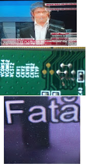
The CSM is a Service Mode that can be enabled by the consumer. The CSM displays diagnosis information, which the customer can forward to the dealer or call centre. In CSM mode, “CSM”, is displayed in the top right corner of the screen.
The information provided in CSM and the purpose of CSM is to:
• Increase the home repair hit rate.
• Decrease the number of nuisance calls.
• Solved customers’ problem without home visit.
Note: For the new model range, a new remote control (RC) is used with some renamed buttons. This has an impact on the activation of the Service modes. For instance the old “MENU” button is now called “HOME” (or is indicated by a “house” icon).
Software Identification, Version, and Cluster
The software ID and version will be shown in the main menu display of CSM.
The screen will show: “AAAAB-X.YYY”, where:
• AAAA is the chassis name: TPS152A x.yyy.
• B is the region indication: E = Europe, A = AP/China, U = NAFTA, L = LATAM.
• X is the main version number: this is updated with a major change of specification (incompatible with the previous software version). Numbering will go from 1 - 99 and AA - ZZ.
- If the main version number changes, the new version number is written in the NVM.
- If the main version number changes, the default settings are loaded.
• YYY is the sub version number: this is updated with a minor change (backwards compatible with the previous versions). Numbering will go from 000 - 999.
- If the sub version number changes, the new version number is written in the NVM.
- If the NVM is refreshed, the software identification, version, and cluster will also be written to NVM.
Customer Service Mode (CSM): Purpose
The Customer Service Mode shows error codes and information on the TV’s operation settings. The call centre can instruct the customer (by telephone) to enter CSM in order to identify the status of the set. This helps the call centre to diagnose problems and failures in the TV set before making a service call.
The CSM is a read-only mode; therefore, modifications are not possible in this mode.
• Ignore “Service unfriendly modes”. • After leaving the Customer Service Mode, the original settings are restored.
• Possibility to use “CH+” or “CH-” for channel surfing, or enter the specific channel number on the RC.
How to Activate CSM
To activate CSM, press the following key sequence on a standard remote control transmitter: from the “Menu/Home screen” press “456987”, directly followed by the “Back” button. (do not allow the display to time out between entries while keying the sequence).
After entering the Customer Service Mode, the following items are displayed.
Note: Activation of the CSM is only possible if there is no (user) menu on the screen
Contents of CSM
Set Type This information is very helpful for a helpdesk/workshop as reference for further diagnosis. In this way, it is not necessary for the customer to look at the rear of the TV-set. Note that if an NVM is replaced or is initialized after corruption, this set type has to be re-written to NVM.
Production code Displays the production code (the serial number) of the TV. Note that if an NVM is replaced or is initialized after corruption, this production code has to be re-written to NVM.
Key (HDCP) Indicates the validity of the HDMI keys (or HDCP keys). In case these keys are not valid and the customer wants to make use of the HDMI functionality, the SSB has to be replaced.
NVM name Detects and displays NVM name.
Software Version Displays the software version.
SW cluster name Displays the software cluster name.
RS232 Display RS232.
TV Region Display TV region.
How to Exit CSM
To exit CSM, use one of the following methods.
• Press the MENU/HOME button on the remote control transmitter.
• Press the POWER button on the remote control transmitter.
• Press the POWER button on the television set.
How to Activate the Factory mode
To activate the Factory mode, use the following method:
• Press the following key sequence on the remote control transmitter: from the “Menu/Home screen” press “1999”, directly followed by the “Back” button. Do not allow the display to time out between entries while keying the sequence.
How to Exit the  Factory mode
Use one of the following methods:
• Select EXIT_FACTORY from the menu and press the “OK” button.
Note: When the TV is switched “off” by a power interrupt, or normal switch to “stand-by” while in the factory mode, the TV will show up in “normal operation mode” as soon as the power is supplied again. The error buffer will not be cleared.
General Alignment Conditions
Perform all electrical adjustments under the following conditions:
• Power supply voltage: 90 - 264 VAC, 50/ 60  3 Hz.
• Connect the set to the mains via an isolation transformer with low internal resistance.
• Allow the set to warm up for approximately 15 minutes.
• Measure voltages and waveforms in relation to correct ground (e.g. measure audio signals in relation to AUDIO_GND).
Caution: It is not allowed to use heat sinks as ground.
• Test probe: Ri > 10 M, Ci < 20 pF.
• Use an isolated trimmer/screwdriver to perform alignments.
 Reset of Repaired SSB
A very important issue towards a repaired SSB from a Service repair shop (SSB repair on component level) implies the reset of the NVM on the SSB.
After a repaired SSB has been mounted in the set (set repair on board level), the type number (CTN) and production code of the TV has to be set according to the type plate of the set.
 SSB Identification
SSB’s of this chassis are identified by a “715” code on the SSB.
715Axxxx-Nnn-MMM-OOOO
• 715 main category, Printed Wiring Board
• Axxxx sub category, sequential coding number
• Nnn Version code
• N Development number
• nn Production number
• MMM Mounting variation code
• OOOO Optional variation code
Make sure when replacing an SSB the SSB identification codes match the replacement board.
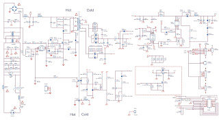
Power Supply Unit
All power supplies are a black box for Service. When defective, a new board must be ordered and defective one must be returned, unless the main fuse of the board is broken. Always replace a defective fuse with one with the correct specifications. This part is available in the regular market.
Consult the Philips Service web portal for the order codes of the boards.
Important delta’s with the TPS15.2A LA classis platform are:
• New power architecture for LED backlight
• “Boost” signal is now a PWM-signal + continuous variable.
The control signals are:
• Stand-by
• Lamp “on/off”
• DIM (PWM) (not for PSDL)
 no detailed information is available because of design protection issues.
The output voltages to the chassis are:
• +12V(on-mode), +8.5V(Stand-by mode)
• +12V_Audio (on-mode),+8.5V_Audio(Stand-by mode )
• +22V for 40", +36V/+24V for 50"/ 55" (bolt-on power) (on-mode)
• Output to the display; in case of
- IPB: High voltage to the LCD panel
- PSL and PSLS (LED-driver outputs)
- PSDL (high frequent) AC-current.
Diversity
The diversity in power supply units is mainly determined by the diversity in displays.
The following displays can be distinguished:
• CCFL/EEFL backlight: power board is conventional IPB
• LED backlight:
- side-view LED without scanning: PSL power board
- side-view LED with scanning: PSLS power board
- direct-view LED without 2D-dimming: PSL power board
- direct-view LED with 2D-dimming: PSDL power board.
PSL stands for Power Supply with integrated LED-drivers.
PSLS stands for a Power Supply with integrated LED-drivers with added Scanning functionality (added microcontroller).
PSDL stands for a Power Supply for Direct-view LED backlight with 2D-dimming.
DC/DC Converters
The on-board DC/DC converters deliver the following voltages (depending on set execution):
• +5V-STANDBY, permanent voltage for the Stand-by controller
• +3V3-STANDBY, power supply for LED/IR receiver and controls
• +12V, input from the power supply for the panel common (active mode)
• +12V, input from the power supply for the amplifier
• +1V5, supply voltage for DDR
• +3V3, general supply voltage
• +3.3V-TUN, supply voltage for tuner
• +3.3V, supply voltage for Headphone AMP
• +5V-USB, input intermediate supply voltage for USB Power
• +3V3 from the power supply for the scaler IC MST6852LP
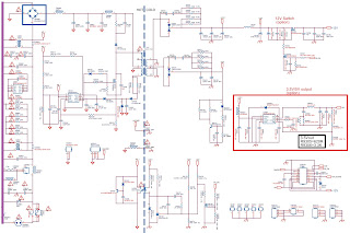
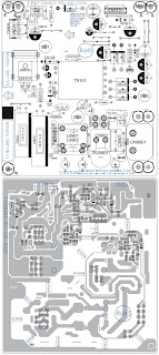
A 715G6934 PSU circuit diagram (Schematic)
Software Upgrading
Description
It is possible for the user to upgrade the main software via the USB port. This allows replacement of a software image in a stand alone set. A description on how to upgrade the main software can be found in the DFU or on the Philips website.
Introduction
Philips continuously tries to improve its products, and it’s recommend that the TV software is updated when updates are available. Software update files can be obtained from the dealer or can be downloaded from the following websites:
http://www.philips.com/support
Preparing a portable memory for software upgrade
The following requirements have to be met:
1. A personal computer connected to the internet.
2. An archive utility that supports the ZIP-format (e.g. WinZip for Windows or Stufflt for Mac OS).
3. A FAT formatted USB memory stick (preferably empty)
Note: Only FAT/DOS-formatted memory sticks are supported.
Only use software update files that can be found on the website.
Check the current TV software version
Before starting the software upgrade procedure, it is advised to check that what the current TV software:
1. Press the “Home screen” + “1999” + “Back” button on the remote control to enter the Factory mode.
2. Use the up/down cursor keys to select “SW Ver”.
If the current software version of the TV is the same as the latest update file found on by the website, it is not necessary to update the TV software.
Download the latest software
1. Open the internet website page http://www.philips.com/support.
2. Find information and software related to the TV.
3. Select the latest software update file and download it to the PC.
4. Insert the USB memory stick into one of the USB ports of the PC.
5. Decompress the downloaded ZIP file and copy it to the root directory of the USB flash drive.
Update the TV software
1. Turn the TV on and wait for it to boot completely.
2. Insert the USB memory stick that contains the software update files in one of the TV’s USB ports.
3. The TV will detect the USB memory stick automatically.
Then a window jumps out.
Note: If the USB flash drive is not detected after power up, disconnect it and re-insert it. And no change the software name.
4. Select [Confirm] and press OK to start software updates.
5. Upgrading will now begins and the status of the updating progress will be displayed. 
6. When the TV software is updated. Remove your USB flash drive, and the TV will turn on automatically.
Note:
• Do not remove the USB flash drive during the software update.
• Do not turn off the power during the software update.
• If a power failure occurs during the update, do not remove the USB flash drive from the TV. The TV will continue the software update as soon as the power comes up again.
• If an error occurs during the update retry the procedure or contact the dealer.
• it is recommended not recommend downgrading to an older version.
• Once the upgrade is finished, use the PC to remove the TV software from the USB portable memory.
Content and Usage of the One-Zip Software File
Below you find a content explanation of the One-Zip file, and instructions on how and when to use it. Only files that are relevant for Service are mentioned here.
• EDID_clustername.zip: Contains the EDID content of the different EDID NVMs. See ComPair for further instructions.
FUS_clustername_version.zip: Contains the “autorun.bin” which is needed to upgrade the TV main software and the software download application.
• NVM_clustername_version.zip: Default NVM content.
Must be programmed via ComPair.
How to Copy NVM Data to/from USB
When copying data to and from a USB memory stick, the folder “repair” is used. When inserting an empty USB memory stick, and downloading data to the stick, the TV will create this folder.
When sending data from a USB memory stick to a TV, the intended data must be available in the “repair” folder.
Note that when copying EDID data to the TV, all necessary EDID files must be in this folder.
Service mode overview for your reference.
Fault Finding and Repair Tips
Note:
• It is assumed that the components are mounted correctly with correct values and no bad solder joints.
• Before any fault finding actions, check if the correct options are set.
No Picture via HDMI input
Check if HDCP key is valid. This can be done in CSM.
TV Will Not Start-up from Stand-by
Possible Stand-by Controller failure. Re-flash the software.
Audio Amplifier
The Class D-IC U601 has a power pad for cooling. When the IC is replaced it must be ensured that the power pad is very well pushed to the PWB while the solder is still liquid. This is needed to insure that the cooling is guaranteed; otherwise the Class D-IC could break down in short time.
Loudspeakers
Make sure that the volume is set to minimum during disconnecting the speakers in the ON-state of the TV. The audio amplifier can be damaged by disconnecting the speakers during ON-state of the set.
Display option code
Attention: In case the SSB is replaced, always check the Panel Code in CSM, even when picture is available. Performance with the incorrect display option code can lead to unwanted side-effects for certain conditions.

Philips 32PHT5100, Philips 40PFT5100, Philips 43PFD5100 – SMPS board circuit diagrams (Schematics)

$
0
0
Philips A 715G6863 PSU, schematic, A715G6863-Component and foils side, A715G6934 PSU schematic, A 715G6934 PSU  LED driver circuit, A 715G6934 PSU component and foil side
Used with: Philips32PHT5100 / 56/79/96/98, 32PHT5100S / 98, Philips40PFT5100 / 56/79/98, 40PFT5100S / 98, Philips43PFD5100 / 30
Used ICs: PF7708AS, PF6003AHS, TK8A65D (FET switch), PF6003AG
Click on the schematics to magnify
A 715G6863 PSU Power board schematic 
A 715G6863 PSU Power board – component and foil side
A 715G6934 PSU – Power board schematic
A 715G6934 PSU – Power board – LED driver circuit
A 715G6934 PSU – Power board component and foil side

Philips 50PFT5100 LED LCD TV – SMPS A715G6955 schematic – Factory mode, Customer service mode

$
0
0
Philips 50PFT5100 / 56/79/96/98, 50PFT5100S / 98, 55PFT5100 / 56/79/98, 55PFT5100S / 98
How to Activate the Factory mode
To activate the Factory mode, use the following method:
• Press the following key sequence on the remote control transmitter: from the “Menu/Home screen” press “1999”, directly followed by the “Back” button. Do not allow the display to time out between entries while keying the sequence.
How to Exit the Factory mode
Use one of the following methods:
• Select EXIT_FACTORY from the menu and press the “OK” button.
Note: When the TV is switched “off” by a power interrupt, or normal switch to “stand-by” while in the factory mode, the TV will show up in “normal operation mode” as soon as the power is supplied again. The error buffer will not be cleared.
How to Activate CSM (Customer Service Mode)
To activate CSM, press the following key sequence on a standard remote control transmitter: from the “Menu/Home screen” press “456987”, directly followed by the “Back” button.
(do not allow the display to time out between entries while keying the sequence).
How to Exit CSM
To exit CSM, use one of the following methods.• Press the MENU/HOME button on the remote control transmitter.
• Press the POWER button on the remote control transmitter.
• Press the POWER button on the television set.
A 715G6955 PSU schematic, component and foil side view: 
Used ICs: AOZ3015AI NC, LD5522, AOTF11N70 (FET switch), PF7909S, AO4440, LD7591T

Viewsonic N2060W Power board 715T 1599-1 circuit diagram [schematic] – 20 inch LCD TV

$
0
0
SMPS circuit diagram [Schematic] - Viewsonic 20 inch LCD TV - N2060W and Thomson 20LW052B5 LCD TVs
Used ICs: FA5500AN, LD7575, STP8NK80ZFP (FET switch]
Foil side
Component side
Schematic
Click on the pictures to magnify

Skyworth 168P-L3L027-K0 SMPS board schematic – TEA1733T-N2, OZ568GN

$
0
0
General description of power supply
This power supply is suitable for 32" LED TV. For 32" LED panel, supplies 4 channels, each channel nominal current value is 90mA; for 32” main board, only supplies +12V power, rated current value +12V/2.5A.
The main part of the circuit:TEA1733T
The main chip of power supply is the TEA1733T which is produced by NXP corporation.The operating mode is CCM (continuous conduction mode), and the operating frequency is 65KHz.
LED driver chip
The chip using OZ568GN, is a highly integrated and high performance LED driver that optimized for LCD backlight application.
Circuit diagram [Schematic] and PWB top and bottom view
Fault Analysis

1. No +12V output voltage
 If there is no +12V output voltage , we should focus on checking the main chip (U6) and judge whether the IC is operating . Monitor its VIN pin and check voltage is normal or abnormal . If it is normal , firstly , check the main chip peripheral circuit . Secondly, check main chip and judge it has broken or not.
2. +12V output is abnormal Check the +12V feedback loop , and the reference voltage of the U3 is normal or not.

Viewing all 2033 articles
Browse latest View live


<script src="https://jsc.adskeeper.com/r/s/rssing.com.1596347.js" async> </script>