↧
AOC 919Pwz - LCD MONITOR - POWER - BACK-LIGHT - SCHEMATIC - (Circuit Diagram)
↧
ViewSonic - VA-703B - VA-703M MONITOR - SCHEMATIC - POWER SUPPLY_BACK-LIGHT INVERTER
↧
↧
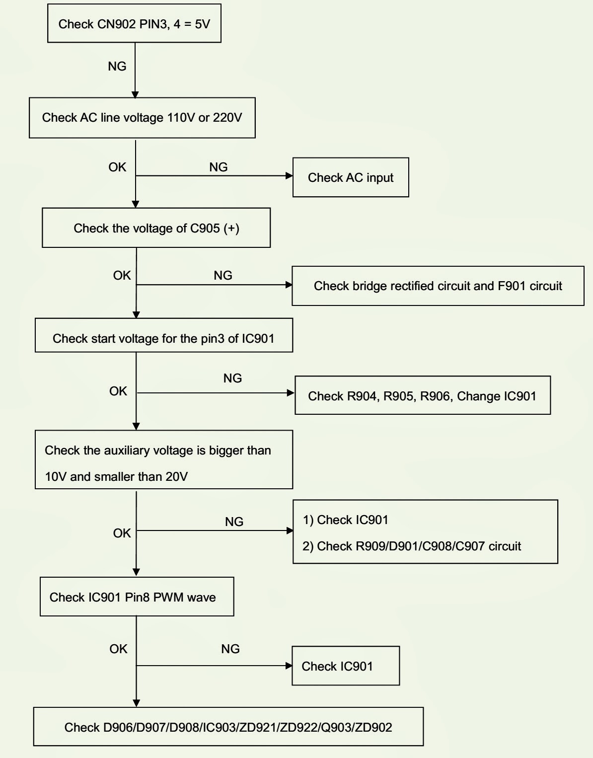
AOC 212VA MONITOR - POWER SUPPLY SCHEMATIC (Circuit Diagram) - TROUBLESHOOTING
↧
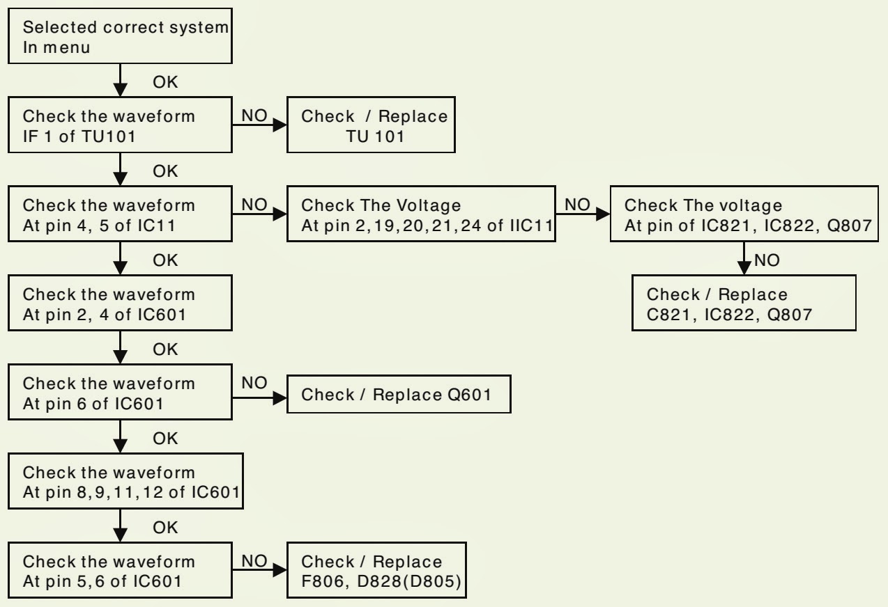
LG CT-20 / 21S45VE/VS _ CT-21S475EX/PX _ TROUBLESHOOTING CHART
↧
SAMSUNG LE17** COLOR MONITOR - SMPS (Power Supply) - SCHEMATIC [Circuit Diagram]
↧
↧
PHILIPS COLOR TV - TE3-2E-CA CHASSIS - SCHEMATIC - POWER - DEFLECTION
↧
SONY TRINITRON - KV 25R** - COLOR TV - SCHEMATIC - POWER SUPPLY [SMPS] - CRT BASE CARD
↧
AIWA NSX S509LX – NSX S514EZ - CIRCUIT DIAGRAM (Schematic) - Compact Disc Stereo Casette Receiver
↧
42ED41 - HITACHI PLASMA TV - VERTICAL LINE - TROUBLESHOOTING
VERTICAL LINE [Troubleshooting]
UNDERSTANDING DEFECT TERMS:
The descriptions below all indicate the particular section which is involved in the abnormality being displayed. Understand that if these lines were only a single pixel in width, then the Panel itself is defective. If the failure is being generated by a PWB and/or a connector, then the line will be at least 8 pixels wide.Address open (line off)
Vertical Influence from the Control,X-Drive Left and Right PWBs and COF.(Note: Defect Line shown is on the front Right, so the X-Drive Left PWB would be involved).
Note: The Screen can be broken down into 7 Vertical Columns. (See the Bottom PWB layout). Each of the connectors from the Control, X-Drive Left and Right PWBs controls each column. Try todetermine which area of the screen is affected to determine the PWB involved. Also, if the COF is defective, the panel is defective and can not be repaired.
Address short (line on)
Vertical Influence from the Control,X-Drive Left and Right PWBs and COF.
(Note: Defect Line shown is on the front Right, so the X-Drive Left PWB would be involved. The Screen can be broken down into 7 Vertical Columns. Each of the connectors from the Control, X-Drive Left and Right PWBs controls each column. Try to determine which area of the screen is affected to determine the PWB involved. Also, if the COF is defective, the panel is defective and can not be repaired.
The figure shows a back view of the Panel.
VERTICAL ADDRESS:
Vertical Addresses is controlled by the COF cables. COF stands for Chip On Film. This means that the Ribbon Cable has embedded IC and resistors.
Note: There are 7 total COF cables controlling the Vertical Addresses. They are broken down into 2, 3, 2. The 2 on the left are controlled by the X-Drive Left PWB, the 3 in the middle are controlled by the Control (LVDS) PWB and the 2 on the right are controlled by the X-Drive Right PWB. The Figure below shows one of the COF cables. Note the chips, capacitors and resistors mounted on the flexible ribbon cables. Also note there are 4 COF per cable. (4 X 7 = 24 COFs). 4 Per cable, 7 Cables.
COF (Chip On Film Cable):
Supplies a waveform which was generated from the Control PWB to the panel and selects a output pin that is controlled by COF (Chip On Film) when it will be on or off. 96 output pin per COF IC.
The higher the resolution, the less spare space where an IC can be placed on the PWB without using IC PACKAGE, so a BARE IC is used embedded right on the cable.
Because IC is not soldered on PWB directly, soldering defect rate is decreased. COF failure requires Panel replacement.
HORIZONTAL ADDRESS:
Horizontal Address is controlled by 6 Printed Circuit Cables. Supplies a driving waveform to PANEL by connecting a PAD electrode of PANEL with PCB
(Y Drive and Z SUS).
There are two types of this for Y Drive PWB. One is single-sided, another is double-side. These have a pattern on it .
For Z SUS PWB, there is no pattern , single-sided and Beta type (all of copper surface).
↧
↧
HITACHI PLASMA TV - 42EDT41 - HORIZONTAL LINE FAULT - TROUBLESHOOT
SUSTAIN SHORT [Line ON]
Horizontal Sustain Influence for Z and Y SUS PWBs, Y Drive Upper and Y Drive Lower PWBs.
(Note: Defect Line shown is on the bottom, so the back X-Drive Left PWB would be involved or the Z-SUS output from the bottom connector).
Note: The Screen can be broken down into 8 Horizontal Rows. (See the Bottom PWB layout) from the Drive PWBs (4 from Upper Drive PWB and 4 from Lower Drive PWB) and 2 Rows from the Z-SUS PWB (Top and Bottom). Each of the connectors from the Control, X-Drive Left and Right PWBs controls each column. Try to determine which area of the screen is affected to determine the PWB involved.SUS open (line off)
Horizontal Sustain Influence for Z and Y SUS PWBs, Y Drive Upper and Y Drive Lower PWBs.
(Note: Defect Line shown is on the bottom, so the back X-Drive Left PWB would be involved or the Z-SUS output from the bottom connector).
Note: The Screen can be broken down into 8 Horizontal Rows. (See the Bottom PWB layout) from the Drive PWBs (4 from Upper Drive PWB and 4 from Lower Drive PWB) and 2 Rows from the Z-SUS PWB (Top and Bottom). Each of the connectors from the Control, X-Drive Left and Right PWBs controls each column. Try to determine which area of the screen is affected to determine the PWB involved.
X DRIVE LEFT AND RIGHT PWB INFORMATION:
Each X Drive PWB Receives LOGIC signals from CONTROL PWB and makes ADDRESS PULSE (generates Address discharge) by ON/OFF operation, and supplies this waveform to COF (data) "Chip On Film".
CONTROL PWB:
This picture shows the Control PWB and it’s 3 connectionsat the bottom to the COF connectors. Creates signal processing (Contour noise, reduction ISM,..) by an order of many FETs turning on/off for each DRIVER. Controls R, G, B (each 8 bit outputs, then parallel split). Uses 3.3V / 5V (2 kinds of power regulators on board ).
CONTROL PWB:
This is a blow up of the Left side of the Control PWB showing the 3.3V and 2.5V Regulators.
↧
TROUBLESHOOTING - HITACHI PLASMA TV - VERTICAL LINE
Symptom was caused by a defective Y-SUS PWB p/n TS05679.
Unit Shuts down after 10~20 seconds. First Power On, 5 sec. later, the Plasma will click, 5 sec. later shutdown.
Found Va voltage loaded 350 ohms or less to ground.
First removed Fuse on the Z-SUS PWB, measure right side of fuse holder as shown in the picture, load disappeared.
Unit Shuts down after 10~20 seconds. First Power On, 5 sec. later, the Plasma will click, 5 sec. later shutdown. Continued…
Traced load out the P1 connector to the Control PWB.
Removed both connector on each side to unload Va. Load disappeared with left side connector P1 lifted. Load remained with right side connector P2 lifted. Found center connector P110 to Panel had the load. Lifted and load removed.
Bottom line, the Panel was defective with a shorted embedded register on the ribbon connector.
DVI Doesn't Work
Clean the DVI input contacts with Isopropyl Alcohol using a stiff thin brush. Sometimes contaminants can cause poor connections on the DVI and/or HDMI inputs.
Cleaning these contacts should eliminate the problem.
LINES or BARS IN THE PICTURE:
The descriptions below all indicate the particular section which is involved in the abnormality being displayed. Understand that if these lines were only a single pixel in width, then the Panel itself is defective. If the failure is being generated by a PWB and/or a connector, then the line will be at least 8 pixels wide.
Address open (line off) Vertical Influence from the Control, X-Drive Left and Right PWBs and COF.(Note: Defect Line shown is on the front Right, so the X-Drive Left PWB would be involved).
Note: The Screen can be broken down into 7 Vertical Columns. (See the Bottom PWB layout). Each of the connectors from the Control, X-Drive Left and Right PWBs controls each column. Try to determine which area of the screen is affected to determine the PWB involved. Also, if the COF is defective, the panel is defective and can not be repaired.
Address short (line on) Vertical Influence from the Control, X-Drive Left and Right PWBs and COF. (Note: Defect Line shown is on the front Right, so the X-Drive Left PWB would be involved).
Note: The Screen can be broken down into 7 Vertical Columns. (See the Bottom PWB layout). Each of the connectors from the Control, X-Drive Left and Right PWBs controls each column. Try to determine which area of the screen is affected to determine the PWB involved. Also, if the COF is defective, the panel is defective and can not be repaired.
SUS short (line on) Horizontal Sustain Influence for Z and Y SUS PWBs, Y Drive Upper and Y Drive Lower PWBs.
(Note: Defect Line shown is on the bottom, so the back X-Drive Left PWB would be involved or the Z-SUS output from the bottom connector).
(Note: Defect Line shown is on the bottom, so the back X-Drive Left PWB would be involved or the Z-SUS output from the bottom connector).
Note: The Screen can be broken down into 8 Horizontal Rows. (See the Bottom PWB layout) from the Drive PWBs (4 from Upper Drive PWB and 4 from Lower Drive PWB) and 2 Rows from the Z-SUS PWB (Top and Bottom). Each of the connectors from the Control, X-Drive Left and Right PWBs controls each column. Try to determine which area of the screen is affected to determine the PWB involved.
SUS open (line off) Horizontal Sustain Influence for Z and Y SUS PWBs, Y Drive Upper and Y Drive Lower PWBs.
(Note: Defect Line shown is on the bottom, so the back X-Drive Left PWBwould be involved or the Z-SUS output from the bottom connector). Note: The Screen can be broken down into 8 Horizontal Rows. (See the Bottom PWB layout) from the Drive PWBs (4 from Upper Drive PWB and 4 from Lower Drive PWB) and 2 Rows from the Z-SUS PWB (Top and Bottom). Each of the connectors from the Control, X-Drive Left and Right PWBs controls each column. Try to determine which area of the screen is affected to determine the PWB involved.
(Note: Defect Line shown is on the bottom, so the back X-Drive Left PWBwould be involved or the Z-SUS output from the bottom connector). Note: The Screen can be broken down into 8 Horizontal Rows. (See the Bottom PWB layout) from the Drive PWBs (4 from Upper Drive PWB and 4 from Lower Drive PWB) and 2 Rows from the Z-SUS PWB (Top and Bottom). Each of the connectors from the Control, X-Drive Left and Right PWBs controls each column. Try to determine which area of the screen is affected to determine the PWB involved.
CLICK ON THE PICTURES TO ZOOM IN
↧
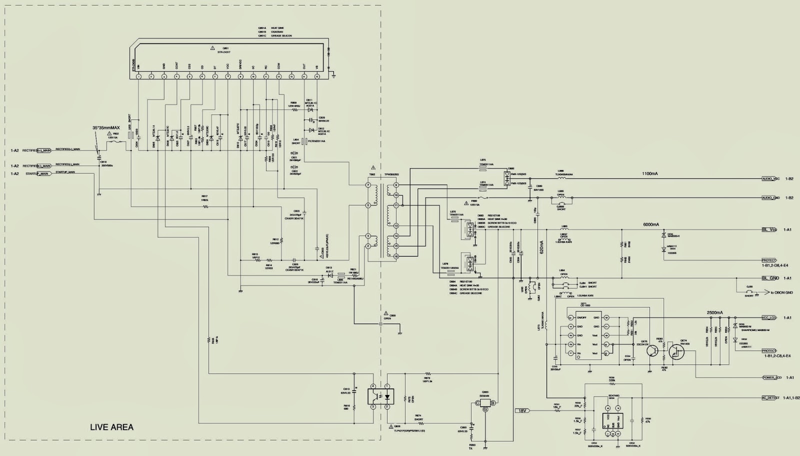
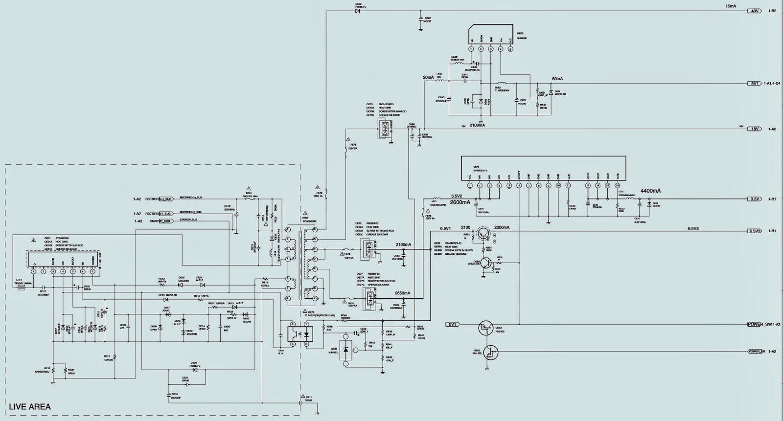
TOSHIBA 32HL95 - LCD TV - POWER SUPPLY [SMPS] SCHEMATIC (STR Z4317)
↧
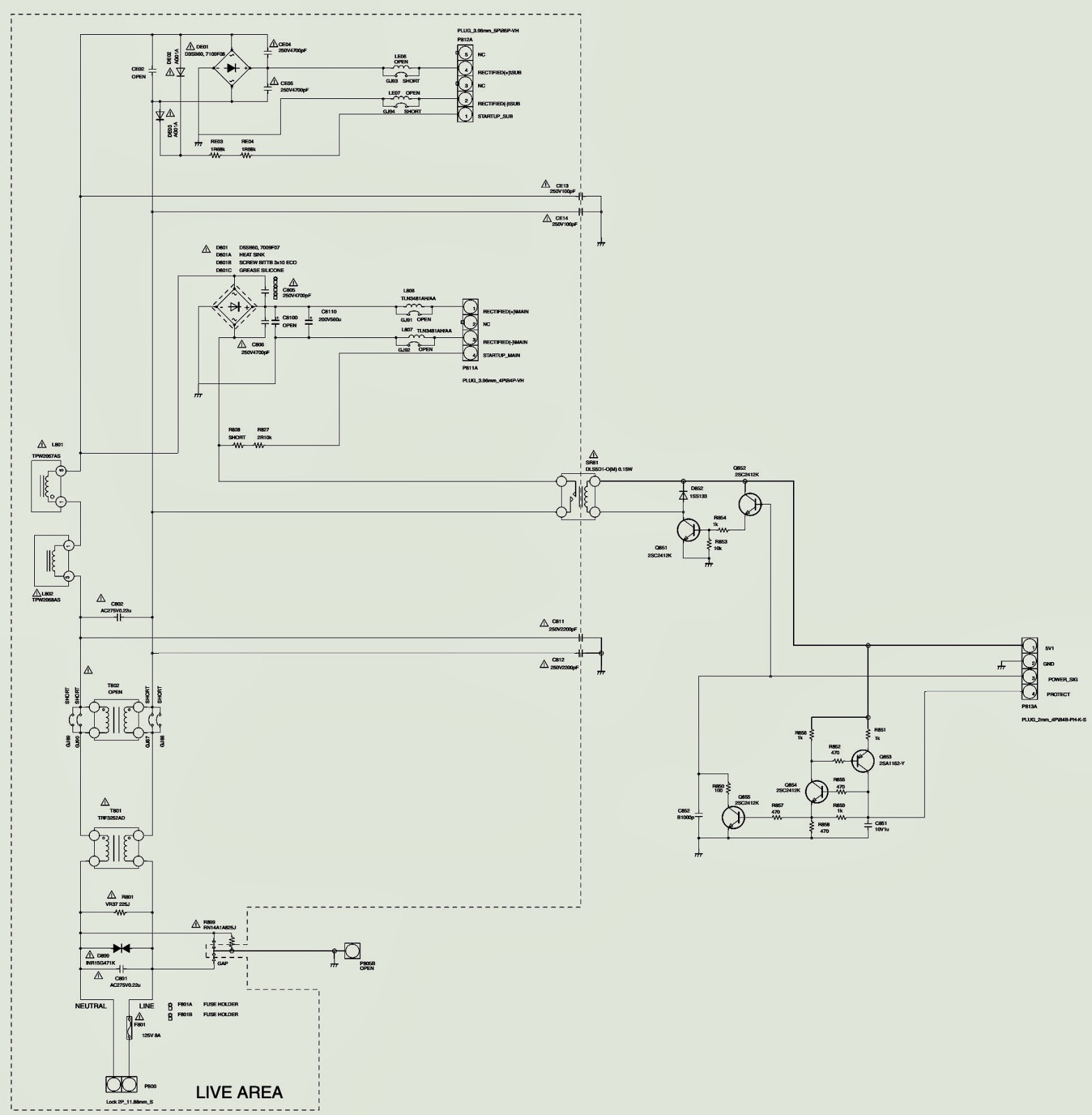
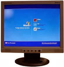
HCL HCM9LWAT11 - LCD MONITOR – POWER SUPPLY SCHEMATIC [Circuit Diagram]
↧
↧
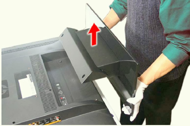
HOW TO DISASSEMBLE PEDESTAL - HP LT3200, LT3700, LT4200, LT4700 - High-Definition LCD TV
PROCEDURE
- Carefully place the TV with the glass screen facing downward on a padded, stable table.
- Position the bottom of the TV near the edge of the table so the pedestal hangs off the edge of the table.
- Remove the four screws.
- Lift the pedestal off the TV.
Disassembling the Pedestal
- Position the pedestal so you can access the screws from the bottom of the pedestal.
- Remove the four screws that hold the two pieces of the pedestal together. Note: Hole usage varies depending on model.
- Separate the two pieces of the pedestal.
↧
ONEAL - [CAXIA] - OCM-600 - SCHEMATIC DIAGRAM (Circuit Diagram)
↧
JBL BP1200.1 - POWER AMPLIFIER - WIRING DIAGRAM [VEHICLE]
↧
JBL BP150.1 - 1 CHANNEL POWER AMPLIFIER - SCHEMATIC (Circuit Diagram)
↧
↧
HOW TO ENTER SERVICE MODE - TOKAI LTVDR-355RF - SMPS SCHEMATIC
SERVICE MODE
- Turn the power on. (Use main power on the TV unit.)
- Press [STANDBY], [2], [7], [1], and [MUTE] buttons on the remote control unit in that order within 5 seconds. When entering the service mode, “4” will display at corners of the screen.
Caution: Optical sensors system is used for Tape Start and End Sensor on this equipment. Prepare as described here before starting to service; otherwise, the unit may operate unexpectedly.
Cover Q202 (START SENSOR) and Q201 (END SENSOR) with Insulation Tape or enter the service mode to activate Sensor Inhibition automatically.
Note: Avoid playing, rewinding or fast-forwarding the tape to its beginning or end, because both Tape End Sensors are not active.
POWER SUPPLY [SMPS] SCHEMATIC
CLICK ON THE PICTURES TO MAGNIFY
↧
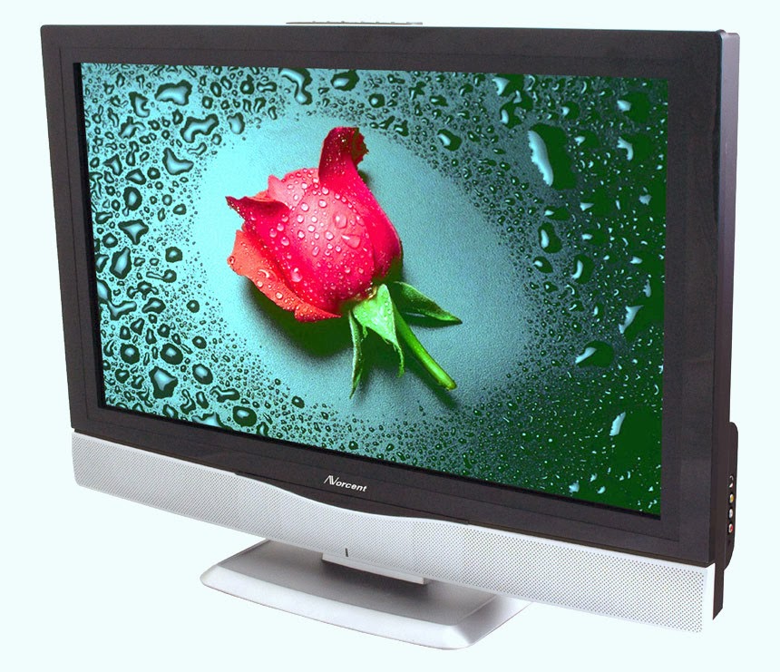
NORCENT [OLEVIA] - LT26HVX-LCD TV - POWER SUPPLY [SMPS] - SCHEMATIC (Circuit Diagram)
↧
HOW TO ENTER SERVICE MODE - MEMOREX MT-1137 - POWER - DEFLECTION - SCHEMATIC
SERVICE MODE
This unit provided with the following SERVICE MODES so you can repair, examine and adjust easily.
To enter the Service Mode, press both set key and remote control key for more than 1 second.
KEY OPERATIONS IN SERVICE MODE
CLICK ON THE PICTURES TO ZOOM IN
CONFIRMATION OF HOURS USED
POWER ON total hours can be checked on the screen. Total hours are displayed in 16 system of notation.
Set the VOLUME to minimum.
Press both VOL. DOWN button on the set and Channel button (6)on the remote control for more than 1 second.
After the confirmation of using hours, turn off the power.WHEN REPLACING EEPROM (MEMORY) IC
If a service repair is undertaken where it has been required to change the MEMORY IC, the following steps should be taken to ensure correct data settings while making reference to TABLE.
- Enter DATA SET mode by setting VOLUME to minimum.
- Press both VOL. DOWN button on the set and Channel button (6) on the remote control for more than 1 second. ADDRESS and DATA should appear.
- ADDRESS is now selected and should "blink". Using the SET + or - keys on the remote, step through the ADDRESS until required ADDRESS to be changed is reached.
- Press ENTER to select DATA. When DATA is selected, it will "blink"
- Again, step through the DATA using SET + or - until required DATA value has been selected.
- Pressing ENTER will take you back to ADDRESS for further selection if necessary.
- Repeat steps 3 to 6 until all data has been checked.
Check if the fixed values of the each adjustment items are set correctly referring below.
SMPS SCHEMATIC
DEFLECTION SCHEMATIC
↧


